|
|
Bachelor's Degree in Telecommunications Systems and in Network Engineering |
|
Lectures and lab sessions |
| Chapter 1: Combinational circuits | ||||||||||||||||
| W1 | L1.1 | L1.2 | Lab1.0 | PLA1 | ||||||||||||
| W2 | L1.3 | L1.4 | Lab1.1 | L1.5 | L1.6 | |||||||||||
| W3 | L2.1 | L2.2 | Lab1.2 | L2.3 | ||||||||||||
| W4 | L2.4 | L2.5 | Lab 2 | L3.1 | PLA1 | PLA2_3 | ||||||||||
| W5 | L3.2 | L3.3 | Lab3 | L4.1 | ||||||||||||
| W6 | L4.2 | L4.3 | Lab4.1 | PLA2_3 | PLA4 | |||||||||||
| W7 | AR1 | Q1-4 | ||||||||||||||
Midterm exam |
Chapter 1 | xx October 2026 (xx:00 - xx:30) | ||||||||||||||
| W8 | Lab4.2 | |||||||||||||||
| W9 | PLA4 | |||||||||||||||
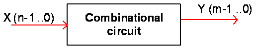 |
Fig. 1. Symbol of a generalised combinational circuit. This block is described by its truth table or the equivalent canonical equations product of maxterms or sum of minterms. |
| Due dates for P_Ch1 post laboratory assignments after having practised in lectures and lab sessions: | ||||||||||||||||
| PLA1 | Due date: 1 Ocober | Circuit analysis using pen & paper (method I), Proteus (method II), VHDL EDA tools (method III) and Wolfram Alpha (method IV). | Q & A | |||||||||||||
| PLA2_3 | 18 October | (A) | Circuit design using single-VHDL file plan A and plan B and multiple-file hierarchical plan C2. Standard arithmetic and logic circuits. | |||||||||||||
| PLA4 | 12 November | Gate level measurements and technology: how fast is a circuit operating? Laboratory prototype FPGA + PCB + measurements. | ||||||||||||||
| Chapter 2: Sequential systems | ||||||||||||||||
| W6 | L5.1 | |||||||||||||||
| W7 | ||||||||||||||||
| W8 | L5.2 | L5.3 | L5.4 | L6.1 | ||||||||||||
| W9 | L6.2 | L7.1 | Lab6 | L7.2 | PLA6_7 | |||||||||||
| W10 | L7.3 | L8.1 | Lab7 | L8.2 | ||||||||||||
| W11 | PLA6_7 | |||||||||||||||
| W12 | ||||||||||||||||
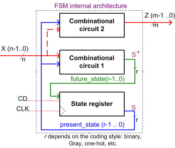 |
Fig. 2. Internal architecture of a synchronous canonical finite state machine as studied in CSD. The state register contains a bank of r D_FF memory cells. r depends on state coding style selected. The FSM, even if structured internally in three blocks, is implemented in a single VHDL file with processes instead of components (the only time where plan C1 is used in CSD). |
| Due dates for P_Ch2 post laboratory assignments after having practised in lectures and lab sessions: | ||||||||||||||||||||||||
| PLA6_7 | Due date: 29 November | (A) | Designing FSM, datapath and dedicated processors | Q & A | ||||||||||||||||||||
| Chapter 3: Microcontrollers | ||||||||||||||||
| W11 | L9.1 | L9.2 | L9.3 | Lab9 | L9.4 | PLA9 | ||||||||||
| W12 | L10.1 | L10.2 | Lab10 | L11 | PLA10_11 | |||||||||||
| W13 | Lab11 | L12.1 | PLA9 | |||||||||||||
| W14 | L12.2 | L12.3 | Lab_AR | AR2 | ||||||||||||
| W15 | AR3 | Q5-12 | ||||||||||||||
Final exam |
Chapter 2 |
Chapter 3 |
xx January 2027 (xx:00 - xx:30) | |||||||||||||
| W16 | PLA10_11 | |||||||||||||||
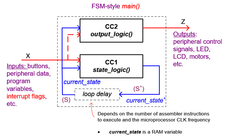  |
Fig. 3. The key concept in Chapter 3 is adapting the FSM structure to software environment in C language. Our programming style and code organisation will mimic concepts studied in previous chapters. |
| Due dates for P_Ch3 post laboratory assignments after having practised in lectures and lab sessions: | ||||||||||||||||||||||||
| PLA9 | Due date 17 December | Microcontroller. Basic digital I/O pins | ||||||||||||||||||||||
| PLA10_11 | 17 January | (A) | Phase #1: Adapting FSM to μC, interrupts; #2: LCD; #3: TMR | Q&A | ||||||||||||||||||||
Key note: PLA2_3, PLA6_7 and PLA10_11 are online submissions at the Atenea platform. Only materials submitted before due dates are considered for grading. To avoid any problems with file types or sizes, please, do not wait until the last minute. Be sure and check that your files can be downloaded and unzipped correctly and also that you include a valid link to your video presentation. Add as well your own self-assessment indicating what grade you might get with respect to our marking guidelines.
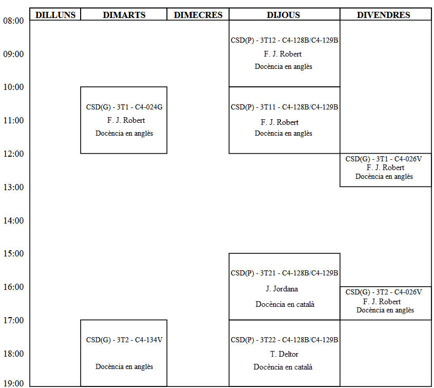
Current term classes and laboratory sessions:
| Home Term 26/27-Q1 Contact Products Electronic devices and companies Software Books Magazines Instruments DEE Library EETAC DEEL |

|
|
| Web activa des de 09/2001, @ F. J. Robert, Web editat amb Microsoft Expression Web 4. El contingut és un complement als materials d'estudi del curs Circuits i Sistemes Digitals disponibles al campus digital Atenea. Llicència:Reconeixement 4.0 Internacional de Creative Commons |