|
|
Bachelor's Degree in Telecommunications Systems and in Network Engineering |
|
Lecture 5 |
L1.5: Designing circuits using only-NOR and only-NAND P1 design plan A: designing circuits using only one kind of gates |
[18 Sep] |
1.5.2.1.3. Only-NOR gates
1.5.2.1.4. Only-NAND gates
These are two strategies or techniques based on simply rearranging the equations for implementing circuits using only one type of logic gate: NAND or NOR.
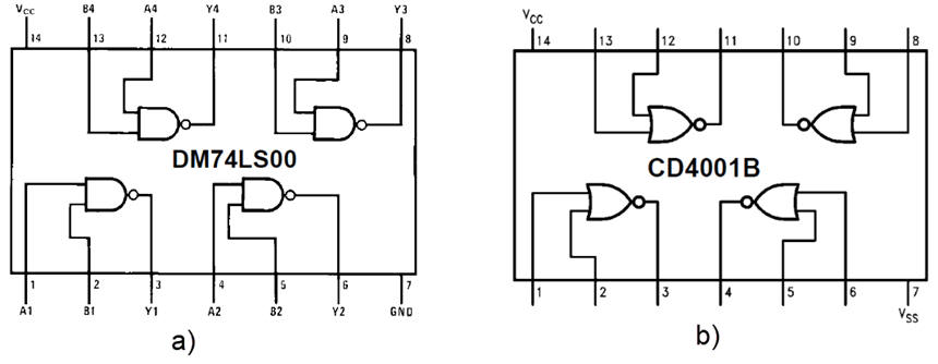
Fifty years ago, it meant being able to implement any combinational application using only one classic chip, such as 74LS00 (quad NAND2, LS-TTL) or CD4001B (Quad NOR2, CMOS). Today the interest of such circuits rely on practicing with Boole's algebra, logic families and technologies.
 |
|
Fig. 1. a) Classic chip 74LS00 (quad NAND2, LS-TTL). b) Chip CD4001B (Quad NOR2, CMOS). |
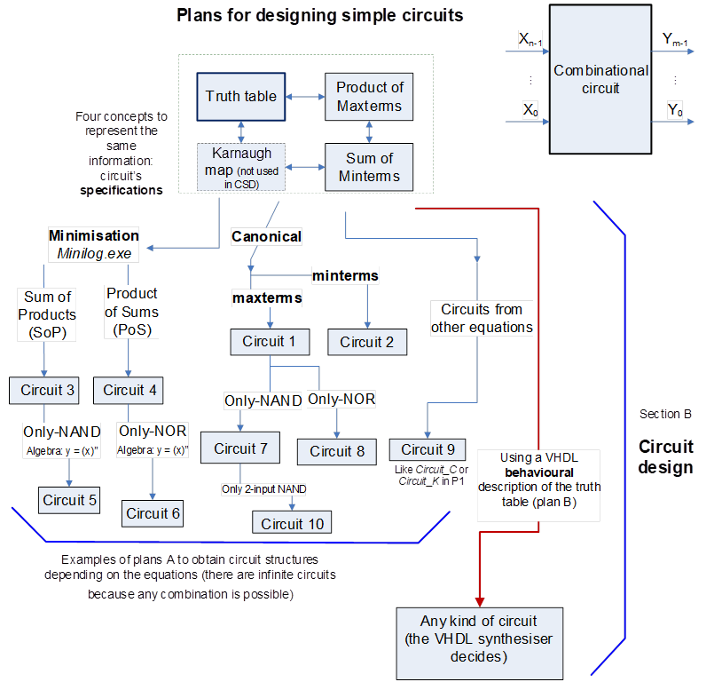
We can add easily these new circuits to our concept map, as any equation can be transformed for only-NAND or only-NOR implementations:
 |
|
Fig. 2. Examples of circuits designed from the initial specifications (truth table). Equations can be modified to invent circuits using only one type of gate: NOR or NAND. |
Now that you know how to use the minimiser Minilog, what is left to finish discussion on P1 design plans is to examine how to build circuits from the same truth table using only-NAND (Circuit_5, Circuit_7, Circuit_10) or only-NOR gates (Circuit_6, Circuit_8).
  |
|
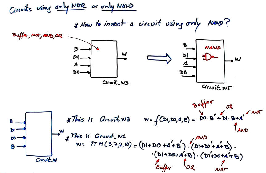
Fig. 3. Class discussion on how to create Circuit_W5 from Circuit_W3. Step1: learn to build any gate using only-NOR or only-NAND. Step 2: learn how to convert a complete equation. Step 3: complete your class-notes and apply these concepts to create other circuits, for instance: how to build Circuit_W11 from Circuit_W3 using only 2-input NOR gates? how to build Circuit_W12 from Circuit_W8 using only 2-input NOR gates? |
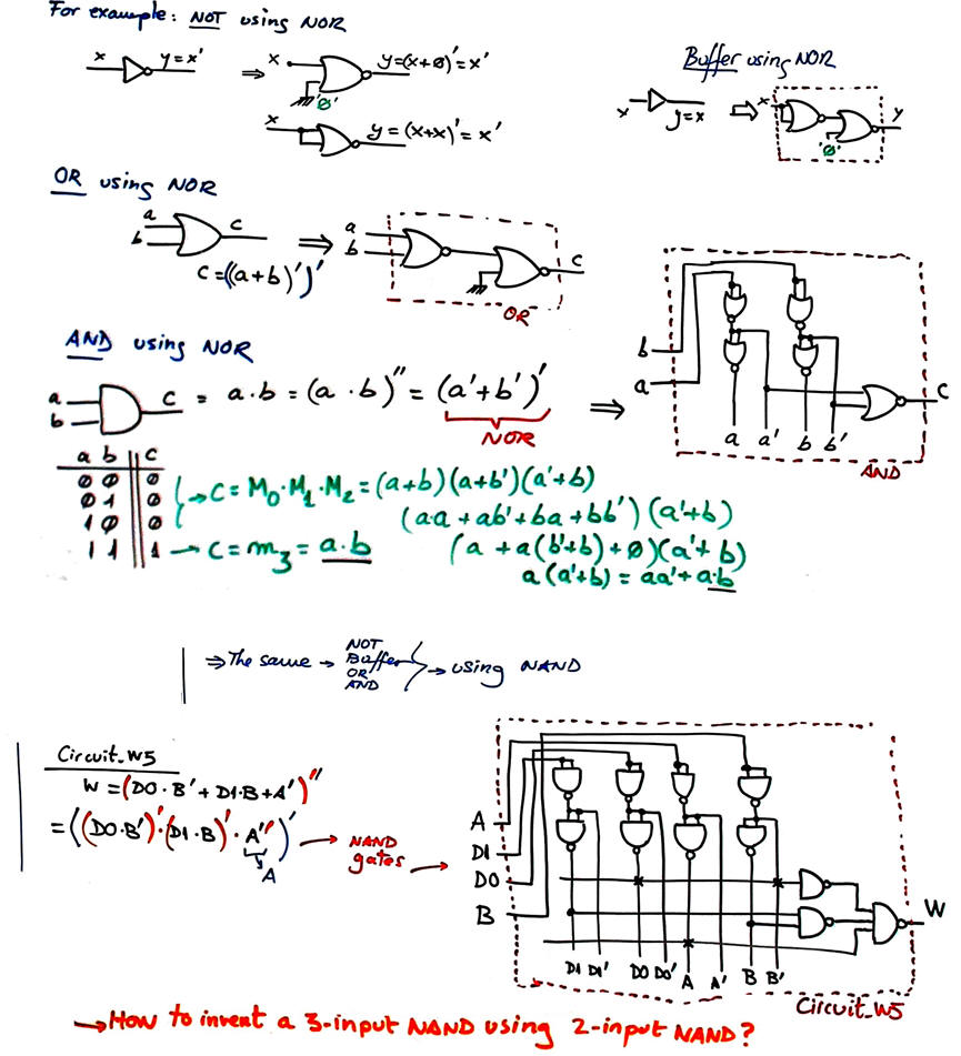
Study also these notes: circuits using only NAND or only NOR gates. This is a trick to use only-NOR2 or only-NAND2 rec.
1.5.2.1.5. Any kind of nonstandard equation.
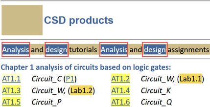
Thus, at this point you see how the many example circuits presented in P1 are conceived mixing any combination of logic equations. CSD course is totally based on similar products, examples and tutorials the link to which is always below specifications of highlighted projects.

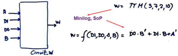
Activity #1: Design the Circuit_W using only NAND of 2-inputs (NAND2). Minimise the truth table using Minilog. Check it using Proteus (CMOS chips, or LS-TTL chips).
Remember: (1) Specifications and theory; (2) Plan in several steps, flowchart, concepts, tools, procedures, etc.; (3) Develop to find a solution for your plan; (4) Test your solution using a given analysis method.
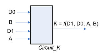
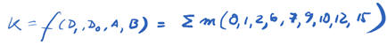
Activity #2: Design the Circuit_K using only NOR of 2-inputs (NOR2). Minimise the truth table using Minilog. Check your solution using WolframAlpha. This Circuit_K3 is a similar tutorial that explain how to build and test the same circuit using only NAND2.
Remember: (1) Specifications and theory; (2) Plan in several steps, flowchart, concepts, tools, procedures, etc.; (3) Develop to find a solution for your plan; (4) Test your solution using a given analysis method.
Activity #3: continue the previous activity #2 in L1.4 designing the circuit Circuit_Z using only NOR of 2-inputs (NOR2).
Alternatively, to complete your training in Boole's algebra, design another time the same Circuit_Z truth table using only NAND of 2-inputs.
Remember that in these activities we do not value final results as we pay attention to project organisation and process dings: (1) Specifications consist of the truth table. (2) Plan in several steps, flowchart, concepts, tools, procedures, etc.; (3) Develop to find a solution for your plan; (4) Test your solution using a given analysis method.
| Home Term 26/27-Q1 Contact Products Electronic devices and companies Software Books Magazines Instruments DEE Library EETAC DEEL |

|
|
| Web activa des de 09/2001, @ F. J. Robert, Web editat amb Microsoft Expression Web 4. El contingut és un complement als materials d'estudi del curs Circuits i Sistemes Digitals disponibles al campus digital Atenea. Llicència:Reconeixement 4.0 Internacional de Creative Commons |