|
|
Bachelor's Degree in Telecommunications Systems and in Network Engineering |
|
L7.1: Counters [P7] Standard sequential blocks: Synchronous canonical counters |
[10 Nov] |
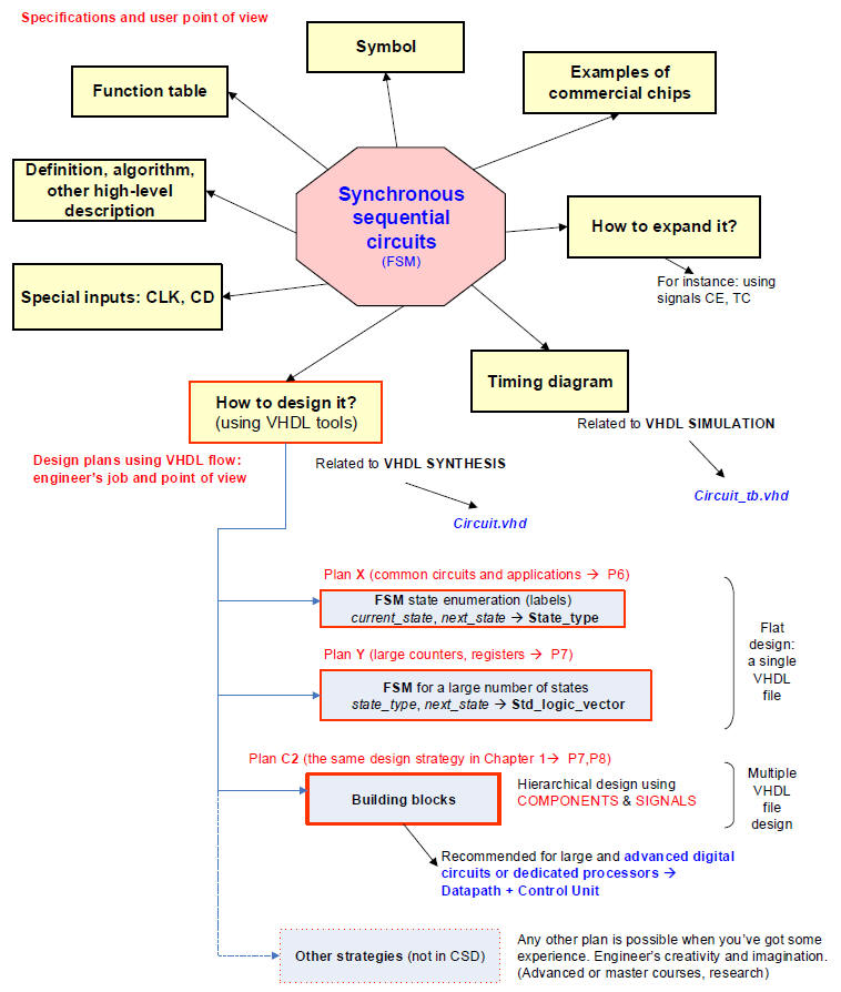
2.7. Standard synchronous sequential systems conceived and planned as FSM
2.7.1. Concept map (pdf)(Visio)
2.7.2. Counters
2.7.2.1. Symbol, function table, modulo, timing diagram, state diagram, commercial chips
2.7.2.2. Control signals: count enable (CE), up and down (UD_L) or reversibility
2.7.2.3. Control signals: terminal count (TC) pulse
2.7.2.4. Output code:
2.7.2.4.1. Radix-2 (binary sequential)
2.7.2.4.2. BCD
2.7.2.4.3. One-hot or one-cold
2.7.2.4.4. Gray, Johnson, etc.
2.7.2.5. Design plan X: designing counters as FSM for small number of states and any output code (single-file plan C1 project) as an enumerated FSM like other examples in P6.
2.7.2.5.1. Example. Run the tutorial: Counter_BCD_1digit
A. Counter_mod12 not controlled (CLK, CD)
B. Counter_mod12 with counte enable (CE) and terminal count (TC12)
C. Counter_mod12 reversible (UD_L)
2.7.3. Radix-2 binary counters (Counter_modM), large number of states
2.7.3.1. Symbol, function table, modulo, timing diagram, state diagram, commercial chips
2.7.3.2. Additional control signal: parallel load (LD) or pre-setting output value
2.7.3.3. Design plan Y: designing counters using the VHDL arithmetic library and STD_LOGIC_VECTOR, single-file VHDL project
2.7.3.3.2. Example. Run the tutorial: Counter_BCD_1digit
2.7.3.3.3. Example: versatile/universal Counter_mod16
Comparison of alternative plans for designing counters. Counter_mod12 with parellel load (LD, Din)
Activity #1: Draw an example timing diagram (pdf) of the binary counter represented by its symbol and its function table.
You may stimulate the entity in your VHDL testbench driving the CLK and the other input signals using processess. A similar timing diagram will be generated by our testing tools, the wave visualiser in ModelSim or or the VB8012 logic analyser in the lab. Hence, you (your cooperative group) will be able to compare solutions and self-detect and correct errors.


Activity #2: Draw the symbol, the function table, an example timing diagram showing the signals and the output codes of a Counter_One_cold_6bit chip. How many states does it have? How to implement it using plan X?, how many VHDL files the project will contain? How many D_FF will contain if states are encoded as an option in radix-2 (sequential), Gray or One-hot?
How to control the counting direction? How to stop (disable) counting?
And another question for the next L7.3: how to implement this Counter_One_cold_6bit using plan C2 using a component Counter_mod16?, how many VHDL files will contain this alternative architecture?
Note: ===> To save and optimise your study time, work in group and ask questions immediately if you have doubts on any of these concepts and proceedings. The final aim is to apply our recipes to design the circuits using VHDL tools for running in FPGA training boards (DE10-Lite, Chapter II; CSD_PICstick, Chapter III).
| Home Term 26/27-Q1 Contact Products Electronic devices and companies Software Books Magazines Instruments DEE Library EETAC DEEL |

|
|
| Web activa des de 09/2001, @ F. J. Robert, Web editat amb Microsoft Expression Web 4. El contingut és un complement als materials d'estudi del curs Circuits i Sistemes Digitals disponibles al campus digital Atenea. Llicència:Reconeixement 4.0 Internacional de Creative Commons |