|
|
Bachelor's Degree in Telecommunications Systems and in Network Engineering |
|
|
|
P_Ch1 Questions and answers |
Consider the discussions in this page as an addendum to your PLA assignments. This edited Q&A come from meet sessions, emails, phone calls, and class and office time with many students. Thus they have significant value and will help you to save study time. You may imagine a class-group working cooperatively in a weekly basis with the objective of solving our projects as better and faster as we can. These are the conditions to participate in Q&A.
-
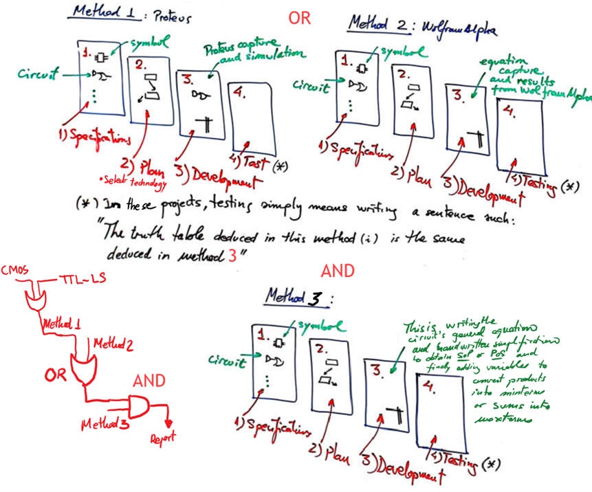
PLA1 Analysis of circuits based on logic gates (method I, II and IV)
Question: I would like to know if capturing the code of Notepad and include it in the development is right or it must be compulsory obtained with the printing option of Notepad++ and place it in the annexes' section?
Answer: This time you simply can paste in a sheet of paper the picture of the coloured text in VHDL that is in you computer screen. And then add some handwriting comments on the picture after printing it to explain details. The same you do when printing and commenting for instance results from WolframAlpha or in this picture showing a section of VHDL from the next LAB2:

Question: I would like to know which combination corresponds to these switch and button states just to be sure for the rest of my work. I think that is "0100" but I am not sure.

Answer: Please, you cannot yet work in your Circuit_L PLA, when you have such questions that are solved running and studying firstly the LAB1_1 tutorial on method II. Ask us what you do not understand from the LAB1_1 circuits first. Everything about buttons, switches and logic values in red and blue ----> please study these concepts in Circuit_W or Circuit C. Be aware that if we detect that you have not developed and run your tutorials projects, we cannot mark your PLA1_1 correctly. In this case on input logic values you must complete the truth table of the Circuit_W.

Question: I just resolved the Circuit_K using method III and checked with Proteus, when I went from the SoP to find the minterms, I had the m2 and m3 twice, I understand that in this case it doesn't affect as it is a sum of minterms. However, if it was the case that I was solving the maxterms, would it affect?
Answer: Well, is your question about a basic property of Boole's algebra from this table? x + x + x + x = x ? yes. If when you try to find a list of minterms using algebra (method 3), you obtain for example: F = m1 + m4 + m5 + m4 + m1 ----> F = m1 + m4 + m5
In the same way, if you are generating handwritten algebraic equations and you get something like this: g = M7 · M8 · M14 · M8 · M6 · M7 ----> g = M7 · M8 · M14 · M6
Question: I have some doubts about the report. I have to do the Circuit_M method 2. In the report I have to do only method 2 and also method 3. Do I have to do it in 8 sheets or in 4? Do I have to put method 1 in the report?
Answer: Instructions tell you to analyse Circuit_M using method 2, this is at least 4 sheets of paper (only after having completed LAB1.1 WolframAlpha project). Instructions tell you to test/check results using method 3, this is another set of 4 sheets of paper. Method 3 is understood as another full project in itself.
Any other project is optional. You always are invited to solve as many of them as you like; digsys contains many exercises. These additional materials can be submitted as well as part of section 1 (specifications and theory) or as annexes.
Question:
1.-When I have the algebraic equation I can't reduce it because it comes out too big.
2.-When I have made the Proteus I get three errors and I don't know why.
3.-When I have done the wolfram equation it does not give me the truth table.
Answer:
1. Step by step. Circuit_W is a section of Circuit_C, and Circuit_C is completely analysed step by step in its tutorial as a highlighted example.
2. One gate at a time and run, this is the way to find where the errors are and correct them. And also discussing your problems with other students.
3. Again, one gate/equation at a time, writing these equations in a file for combining them and running them in WolframAlpha. Learn WolframAlpha using LAB1_1 session materials.
Question: In WolframAlpha, can I change some variables indicating what is each one in the case that I change it in the report? For example: T = A and, X0 = B ?
Answer: Yes, if you clearly explains what you are changing and you are able to identify maxterms and minterms correctly from WolframAlpha results. Your report MUST have original symbol names. However, if possible solve all CSD exercises without modifying directories, entity, input or output names. In WolfraAlpha you can reorder expressions and even use other parenthesis styles like [ ] or { } to represent clearer expressions.
For example: logic circuit not{ not(not(X1) or [T xor Q]) or not(X0 or not (X1) ) }
You can also use mathematics language symbols instead of natural language for writing your circuit general equation, as WolframAlpha itself does when interpreting your text inputs.
For example: truth table (Q xor T) and X0 -----> truth table (Q xor T) && X0
NOT --> ~ AND --> && OR ---> ||
logic circuit not{ not(not(X1) or [T xor Q]) or not(X0 or not (X1) ) } --->
---> logic circuit ~ ( ~ (not(X1) or [T xor Q]) or not(X0 || not (X1) ) )
Question: I'm having some trouble on trying to extract the circuit N's truth table, I'm doing it through method 1. The point is that when I extract the truth table from simulating on Proteus I got six minterms, but when I try to extract the truth table with the method 3 I have also six minterms but not the same from method 1. I'm trying to find the error but I just can't see it.
Answer: If you have done the processes for solving both projects is OK, your PLA will get a good mark. Now, the final result is not that important, project processes count much more. Next week you will be asked to solve the same circuit with the other two methods remaining, and in this way, you will be able to identify better where your errors are located. Or even better, talk to your team or class mates to be sure which is the sum of minterms for your circuit.
Question: En acabar el PLA1_1 i com m'agradaria enquadernar-lo li volia demanar a veure si és possible utilitzar 13 cares (una cara per fulla) perquè quedi més net el resultat en lloc d'utilitzar 7 fulles a doble cara. Sé que el màxim són 8 fulls a doble cara però tenint en compte que el que he fet no s'excedeix, volia comprovar si és possible fer-ho.
Answer: The minimum paper per project is four sheets, and add as many sheets as you need. For example, you may like to add as much theory, class notes or exercises as you want or as you need at section 1 accompanying the specifications. We are only asking you to prepare each project using the given four sections. And do not prepare book covers or embellishments or improvements for your submitted work. We are only interested in your draft solution and in how you are completing the process of analysing circuits. This kind of improvements, like covers, or using a word processors or Visio for pictures and schematics, is something that you will do for other courses or in your final dissertation.
Question: We have been told to do 4 pages per method every time we analyse a circuit. But when printing it, can we print them in both sides of the paper? It's a very good way to reduce the amount of paper and to preserve the ink of our printers which is very expensive.
Answer: Every project section is a new sheet of paper not a page side of paper. Don't worry now about the cost of some sheets of paper. The ink is preserved using white background, be careful to change colours in all pictures printed. Instructions are given on how to do it in ModelSim, and in any other software you can use any application for drawing to change colours and get them lighter to save ink. Most of the pictures found in digsys are examples of light/white backgrounds. Do not use word processors for writing comments on pictures or annotating, because only handwriting is accepted. Projects have four sections, but they may contain more that four sheets, for example a long development, or a project specification including also theory.
Question: I am writing to inquire about this week lab session. Could you please confirm if there are any specific tasks to be completed beforehand, or if we will be working on the lab during the session and submitting a report in the following one?
Answer: In lab sessions we follow tutorial materials described in the corresponding session. For instance, this is what we will do the next LAB1.1. In this first session, we will require you to have installed correctly Proteus in your portable computer in order to analyse the proposed circuit using method II.
Preliminary work is not necessary; we have concluded that it is much better to ask you to solve during the week a post-lab assignment, the PLA1 indicated by your instructor, a similar project to the one proposed during the lab session. You will submit it in paper and in the format that we use for projects during the next LAB1.2 session, in this case, by September 26, as indicated in our timetable.
However, because everything to do during the course is online and available for discussion, you can ask any time as many questions as you like. Or study ahead of classes and labs. No problem.
Question:
Answer:
-
PLA1 Analysing circuits using VHDL synthesis and simulation EDA tools (method III)
Question: How to replace default background black colour in ModelSim wave timing diagrams?
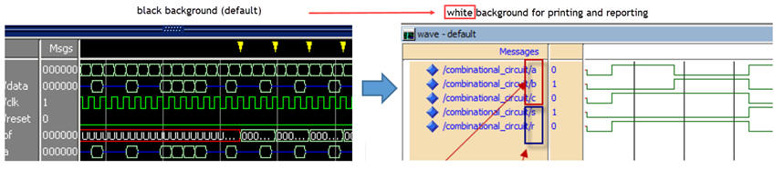
Answer: In this EDA page there is the document explaining how to do it once ModelSim is installed in your PC.
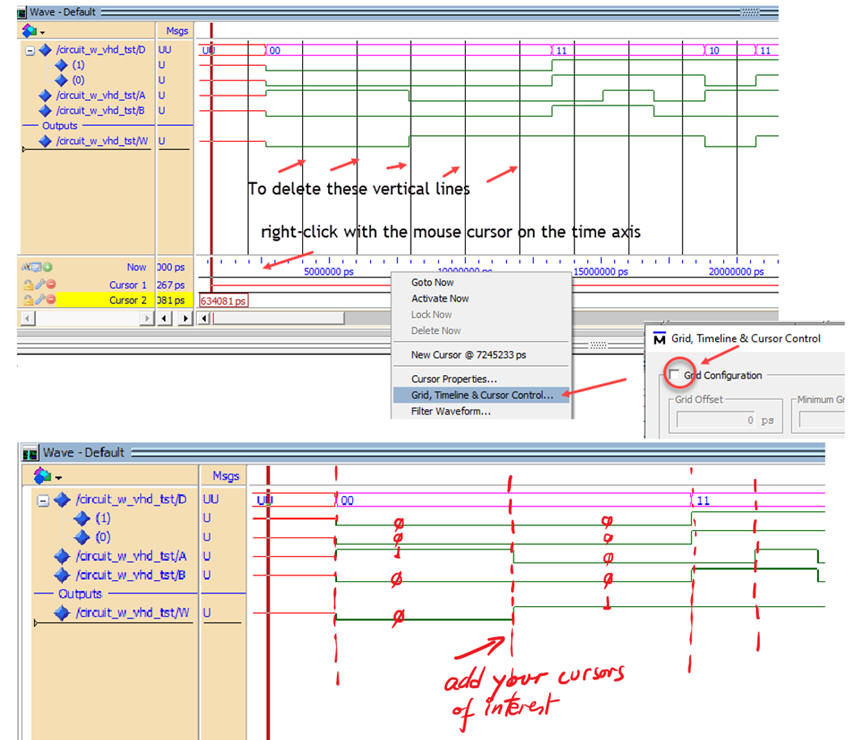
Question: How to eliminate vertical grid lines in ModelSim wave diagram, so that writing comments is easier and the picture cleaner?
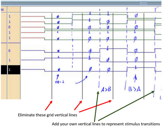
Answer: This is how to deactivate the default grid, so that you can add your own vertical lines to indicate signal transitions or edges.
Question: I was modifying the "Circuit_W_tb.vhd" file to fit my circuit. When we begin the stim_process, do we need to include all 16 combinations in it?
Answer: Ok, follow the step-by step note guidelines indicated at PLA1. Lab1_2 tutorial on Circuit_W analysis must work correctly in your computer before thinking on anything else.
No, when you start simply add two or three combinations, because the objective in this step is to check whether you can get results from ModelSim wave diagrams. When everything works fine, you can edit the testbench file again and add all the combinations because your objective is to write down the truth table.
Question: What Min_Pulse do we define? Is it up to us to decide?
Answer: Yes, any time constant is Ok. If for instance you choose Min_Pulse = 3.3 ms, you will run the simulation for 600 ms, enough time for applying all vectors defining the full truth table.
Question: When compiling both files in ModelSim, the tb gives me an error. Is there any way to know where is it? Could it be just a semicolon? If that is the case, how do we know when to write a ':' or ';' or ',' or nothing?
Answer: This is why we ask you to follow the step-by step indications. In our testbench for Circuit_W there is no errors. Thus you simply study and adapt vectors and everything else from another similar example. In this way, there is no need to pay that much attention to VHDL syntax.
Question:
Answer:
Question: I'm attaching in this email my VHDL file, it tells me that I have to buffer the CHs, what command allows me to change the CHs to buffers? Another issue is that I don't know if I have the correct VHDL, can you tell me where it would be wrong or what I can improve?
Answer: 1) Run the projects and and study our lab2 materials in your computer, and only when everything is working fine, start thinking in PLA2_3 specifications. 2) Study several examples of plan A and plan B circuits from out lessons and tutorials in DIGSYS. 3) Study circuit symbol, truth tables and timing diagrams (section 1 : specifications). 4) Propose an schematic/flowchart/diagram(etc. for your design in paper, and if you have questions on how to translate it to VHDL, show us your schematics in emails or meet sessions or even better attending our lectures. In CSD, VHDL files are only direct translations of your diagrams and schematics, there is no need to discuss VHDL files.
Question: Is this report page on Minilog results correct for our report?
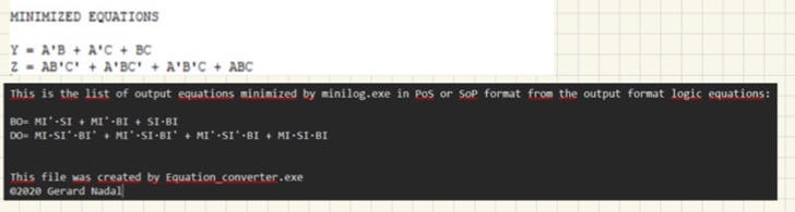
Answer: No, please NEVER print or show us anything using black background, it will simply downgrade your PLA's. Do whatever necessary to have ALWAYS white background from all your pictures. Besides, if you are trying to show results from a Minilog minimisation, you must write down the equation in paper, which later in the development section will be exactly translated into VHDL using another text file (*.vhd).
-
PLA2_3 Designing arithmetic and logic circuits using plans A, B and C2
Question: We are a lab group of three students, what is the meaning of these instructions? How many projects do we have to to implement?

Answer:
Yes, a group of three students should be able to solve three projects to learn about our plan A, B and C2 ways of inventing circuits to be developed and tested by means of VHDL tools.
Yes, you will use the D1.1 and try to solve it using equations PoS (plan A); this is inputting the truth table in Minilog and generating the 23 output equations. You can do it in several steps, for instance, firstly generating only Y(15..0) and develop and test in VHDL. And only when it works, you can add the additional segment S(6..0) outputs to the same project to complete the design.
One of the components included in the ALU_12bit (D1.18) is the Doudecuple_MUX_4 that can be planned in different ways, but better if you use it for practising plan B, which is much simple; similar to other plan B multiplexers available in digsys products. [A similar circuit can be found in this ALU_9bit to be used in the next LAB4.2].
The ALU_12bit is completely designed/planned in the problem D.18 in several layers of components as we practised in LAB3 and LAB4.1. The idea is to translate it all into VHDL as a plan C2 exercise. This top ALU_12bit circuit includes the component Adder_4bit from which we have two versions, thus use the Adder_4bit with the internal carry-lookahead architecture (CLA).
Question: We are in charge of solving using plan C2 the D1.19 on a parking occupancy system of 31 slots, and also the 5-bit ones counter in D1.3. We have three questions:
1. On specifications, for the plan C2 do we have to write all the truth table or simply some combinations will be enough?
2. On the planning, how to deduce the internal circuit of the parking_occupancy?
3. On the video: how to organise the 10 min. presentation in group? How many project we have to explain, a single project or all three?
Answer:
1. Have you found other similar circuits to imagine how will be your specifications like the highlighted P3 ? Show simply some values of the truth table, as indicated in the test vectors, (the full table is huge, 2 raised to the power 36 !! ). You have to try some vectors, start with some of the number of ones and reserved slots given to you as option, and if you need more numbers, add then to your timing diagram. The idea of the timing diagram is to clarify the truth table and be able in section 4 to translate it as a process for your VHDL testbech fixture in ModelSim.
2. The key point is on applying plan C2: how to design such large circuit using smaller components of the same kind and other blocks like adders? You may like to use your Ones_counter_5bit several times.
You may like to propose your plan in several steps. For example, the outputs are directly 7-segments active-low. Thus, you can imagine in a step #1 a circuit with binary outputs and complete the project (and only the parking slot inputs). And only when is working and you have tested it, you can add the step #2 connecting the converters, from binary to BCD, and from BCD to 7-segments, or something like this. In another final step you can add the reserved slots. In this way, the truth tables are going to be easier to imagine, and you will complete partial projects. Remember that there is no need to complete it all by the due date, this PLA2_3 is continued in PLA4.
3. Your lab instructor will tell you specific instructions on how to organise the presentations. The general guidelines and some notes for video presentations are similar for all subjects, so CSD is not different, you are practising a cross-curricular skill. And we have up to three opportunities (PLA2_3, PLA6_7 and again in PLA10_11) for improving them using our feedback on how you did it. A good idea to start is recording a meet session including your live images and presenting slides with significant schematics and diagrams. Once done, upload it in your drive and send us simply the link with permission to watch it.
10 minutes presentation and three students give you several options, all of them valid. For example:
(1) Choose and present between you three a single project (the one in plan A or in plan B or in plan C2). They have up to four sections each, so presenting in detail the sections in two o three minutes is a good idea.
(2) Present each of you a full project, thus in 3 minutes you should explain a bit of everything of each project.
(3) Present de projects more cooperatively, interacting and intervening several times each of you in the 10 minutes slot; but this requires more practice. Better leave it for the PLA10_11.
(4) Etc.
Question:
Answer:
Question:
Answer:
Question:
Answer:
-
PLA4 on gate-level measurements (how fast is a circuit calculating?)
Question: In the specifications of the PLA4, there is this task: - Demonstrate that the circuit does not calculate correctly when Min_Pulse is shorter that the circuit's propagation delay. In my case, the max propagation delay obtained from Quartus Prime is xx.yy ns and the one obtained in ModelSim with my test numbers is zz.ww ns. Just to demonstrate the results is enough? Or, do I need to create a bigger Min_Pulse than xx.yy ns and run again?
Answer: In ModelSim you are calculating propagation delays in a given transition of the many, not necessarily the worst-case scenario. Using timing analyser you calculate all propagation delays from any input to any output, thus being able to measure the longest path. For instance tP = xx.yy ns in your case. We are asking you now to run a gate-level ModelSim simulation considering a constant Min_Pulse < tP so that you are forcing your circuit to switch faster than it can, and probably you will see on ModelSim waves that outputs are not reaching stable values with correct calculation results.
Question: Concerning the report of PLA4, can we reuse the same report as in PLA3 adding the fifth section (gate-level simulation)?
Answer: Well, yes, optionally, you can photocopy the 1-2-3-4 report from LAB3, modify something if you need it, from the given feedback or perhaps because your PLA3 was not yet fully working, and then add your design step 5 (individual). At least two sheets, because you are working with two new tools: gate-level simulation in ModelSim and Quartus Prime timing analyser. But, before anything else, you have to ask and discuss these report ideas and details with your lab instructor. Study and develop all the LAB4 project in your computer before starting this PLA4.
-
PLA4 prototype, lab measurements, instruments
Question: I would like to ask you a question about the PLA4_2. Is it a full project with typical sections 1-2-3-4? What must include about the LAB4.2 session? And all the exercises of Exam 1 must be solved?
Answer: Simply some pages with answers to the questions, this PLA is not a full project. The project ALU_9bit is already fully reported in the page LAB4_2 including also the real prototyping and measurements section. The LAB4_2 is focused only on these measurements and practical prototypes even if all the project is included.
There is a question about the specifications of the ALU_9bit, its truth table, how to operate as it was asked in the Exam1 P1. We want you to try to solve the exam problem P1, midterm is a good time to review these materials. And, as we always say, it is a very good idea to see if you can solve not only this exercise, but all the exam. It is midterm, and thus plenty of time for solving questions and comprehending circuits.
And the other questions are about what you measured or annotated during the session or if you did some other pre-lab questions as well that you like to report.
Question: In questions 4 and 5, we don't have lab screenshots or class notes, it says 'discuss how this value can be inferred,' but we're not exactly sure what we need to do.
Answer: In L4.3 we discussed in class approximate ways to explain the theory behind speed and power consumption in logic gates. And the full project LAB4_2 explains in detail how some measurements are performed for real using instruments and experiments. Imagine that you are using these questions for studying to solve exams, like if you were studying for solving the last Exam1 questions on speed and power.
| Home Term 26/27-Q1 Contact Products Electronic devices and companies Software Books Magazines Instruments DEE Library EETAC DEEL |

|
|
| Web activa des de 09/2001, @ F. J. Robert, Web editat amb Microsoft Expression Web 4. El contingut és un complement als materials d'estudi del curs Circuits i Sistemes Digitals disponibles al campus digital Atenea. Llicència:Reconeixement 4.0 Internacional de Creative Commons |