|
|
Bachelor's Degree in Telecommunications Systems and in Network Engineering |
|
Lecture 4 |
L9.4: Basic digital I/O. Write output port pins [P9] truth_table(), write_outputs() |
[27 Nov] |
3.4.2.2.4. truth_table(), behavioural description (plan B), algorithm
The same algorithm and ideas presented in Chapter 1: plan B: behavioural truth table interpretation that now will be translated into C language. Two example circuit truth tables are presented in P9 (Fig. 11) and LAB9. (Fig. 11).
Thus, once again, you see how the same combinational circuit entity can be yet designed using another plan in the list: implementing logic functions using microcontrollers and software programing (strategy number 9).
3.4.2.2.5.write_outputs()
Our goal: How to interface RAM memory bits to output pins? From '0' and '1' stored in internal RAM variables, write the 8 pins of a PORT in a single instruction without modifying the data available in pins of no interest. For instance, write var_TC10 to RB2; write var_BCD_Units to RC2, RB5, RB4 and RC0 as shown in Fig. 1
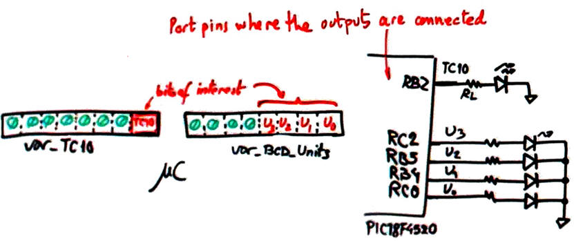 |
Fig. 1. Let us write/extract/output RAM variable values in port pins. |
Our plan: Use bitwise logic operations (AND, OR, XOR, NOT, SHIFT, etc.) executed by the μC's ALU to output variables logic values into specific port pins where the signals are connected.
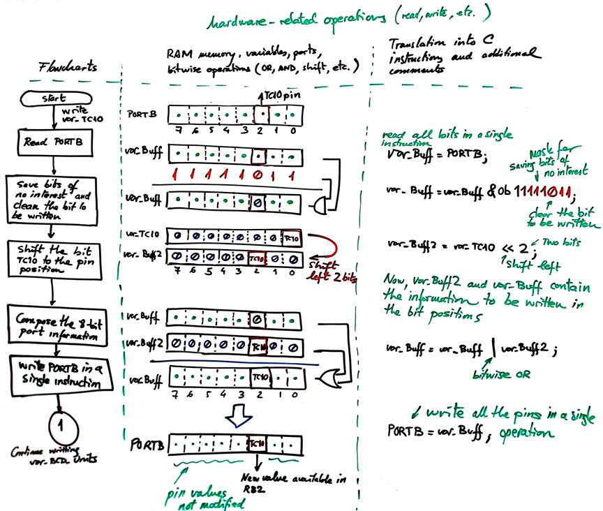
Fig. 2 is an example planning sheet on how to write a single bit variable like this var_TC10 connected to a μC pin (RB2). In this way it is easy to deduce which C instructions are required in the source file.
 |
|
Fig. 2. Example on how to write a single output pin. |
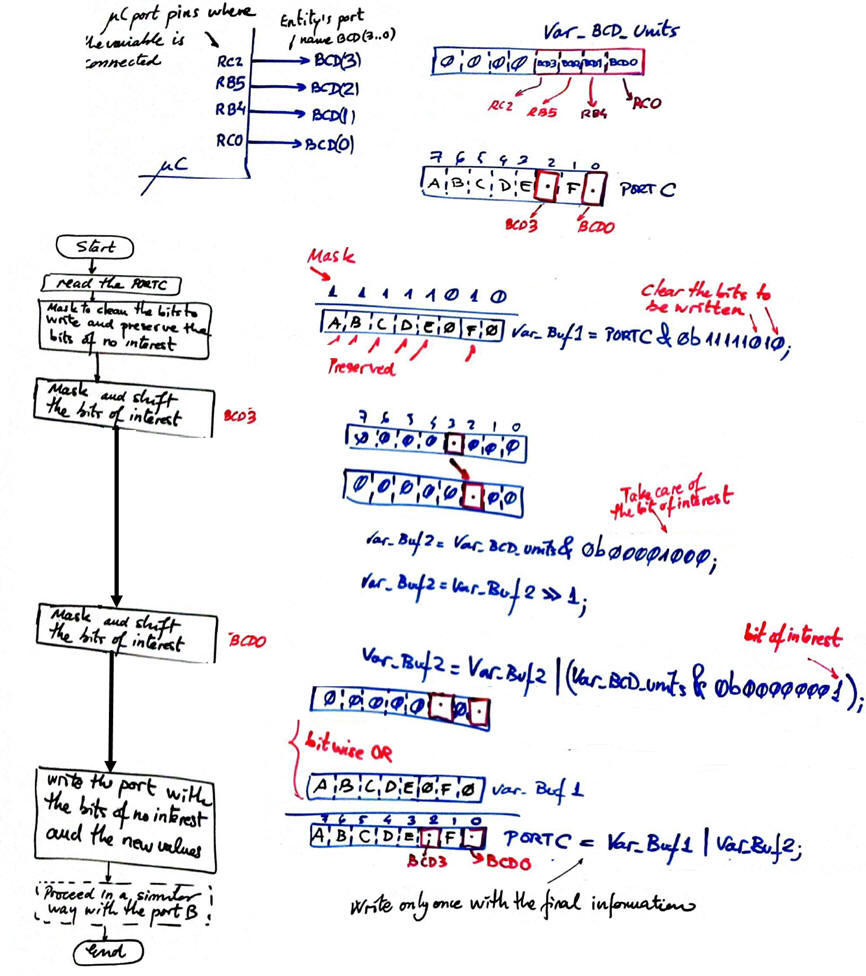
Fig. 3 is an example planning sheet on how to write a vector variable like var_BCD_Units connected to μC pins in two different ports. In this way it is easy to deduce which C instructions are required in the source file.
 |
|
Fig. 3. Example on how to write a vector variable onto several port pins. Repeat the same proceeding for var_BCD_Units (2..1) at PORTB. |
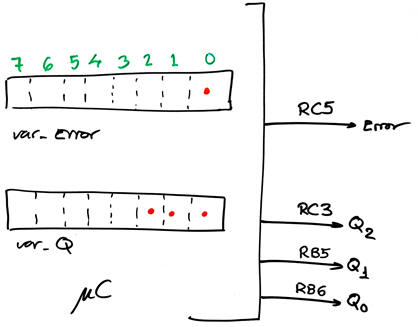
Activity #1: Explain in a three column sheet the flowcharts, the memory bitwise operations and the C instructions for writing variable var_Error at pin RC5, and var_Q at pins RC3, RB5 and RB6.
Activity #2: Write an output pin from your assigned PLA9 circuit. Explain in the three-column report sheet proposed in this unit (Fig. 2, Fig. 3), the flowcharts, content in RAM memory variables, bitwise operations and C code translation for converting RAM variables into voltages available at port pins.
If you work in teams, each group member writes a different output.
| Home Term 26/27-Q1 Contact Products Electronic devices and companies Software Books Magazines Instruments DEE Library EETAC DEEL |

|
|
| Web activa des de 09/2001, @ F. J. Robert, Web editat amb Microsoft Expression Web 4. El contingut és un complement als materials d'estudi del curs Circuits i Sistemes Digitals disponibles al campus digital Atenea. Llicència:Reconeixement 4.0 Internacional de Creative Commons |