|
|
Bachelor's Degree in Telecommunications Systems and in Network Engineering |
|
Lecture 2 |
L2.2: Designing standard logic circuits using VHDL. Multiplexers, demultiplexers [P2] Flat (single VHDL file) plans: structural plan A / behavioural plan B |
[22 Sep] |
1.7.2.2. Design examples (our list of design strategies)
Alternative ways to invent circuit architectures in VHDL:
Plan A) Structural (flat) - one VHDL file using equations. Used from P1.
Plan B) Behavioural (flat) - one VHDL file using the truth table, algorithm or flowchart.
Plan C1) Structural (hierarchical) - describing a hierarchical structure in a single VHDL file (complicated and not recommended- We will use it only in P6 to describe a FSM in a single file).
Plan C2) Structural (hierarchical) - several VHDL files using COMPONENTS, SIGNALS and logic equations. This modular approach is the best at CSD introductory level to design large circuits. Introduced in next P3.
1.7.3. De-multiplexer or data distributor
Specifications Design a DeMUX_8 circuit.
What is the application of a DeMUX_n? The idea is to send data from a single source to different destinations. This is an example of MUX_DeMUX.pdsprj circuit simulation.
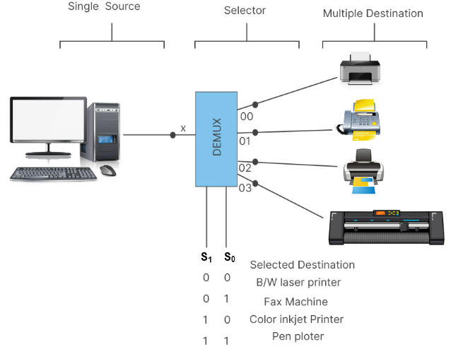 |
| Fig. 1. Typical application of data distributors. |
1.7.3.1. DeMUX_4, DeMUX_8, etc.
What is the symbol and circuit's truth table of a DeMUX_8? Draw a timing diagram. Find an example commercial chip.
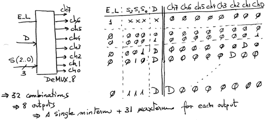 |
| Fig. 2. DeMUX_8 symbol and truth table. |
Plan
1.7.3.2. Design examples using plan A and plan B.
Several circuits can be implemented using our project planning and organisation for VHDL EDA tools, depending on the plan. For example:
- Plan A: examine the truth table in Fig. 2. Deduce the equations using ones (minterms), which is much easier and practical than writing the dual equation using zeros (maxterms). Or, instead, write the truth table file "DeMUX_8.tbl" and run Minilog to find directly the minimised SoP or PoS for each output. Synthesise the circuit for a given target CPLD or FPGA chip and check it using a VHDL testbench (as we propose in these LAB1.2 or LAB2 tutorials).
- Plan B: capture the circuit's algorithm in a flowchart or adapt the truth table as an schematic as shown in Fig. 3. Translate it into VHDL and synthesise the circuit for a given target CPLD or FPGA chip and check it using a VHDL testbench (as we propose in these LAB1.2 or LAB2 tutorials).
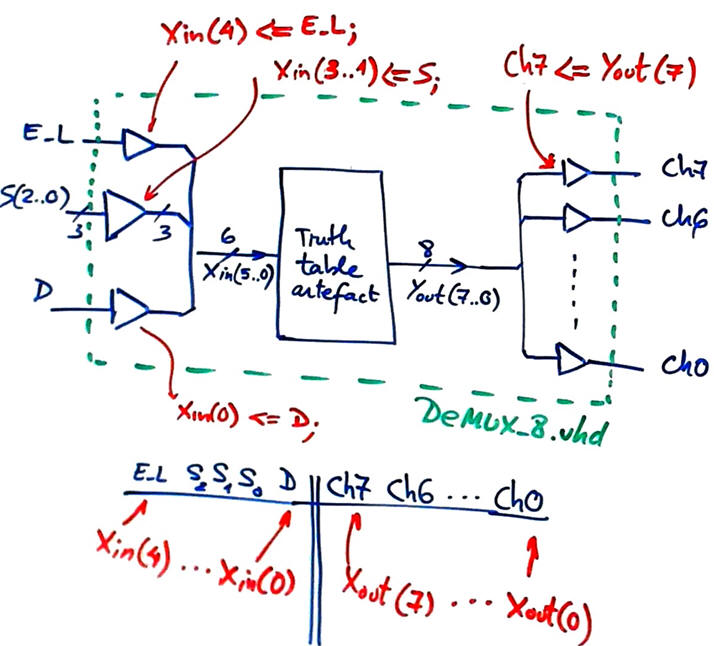 |
| Fig. 3. Example schematic ready for VHDL. We do not provide equations or circuits, but translate the complete truth table using VHDL statements and artefacts. The synthesiser will find a convenient circuit ready for implementation in FPGA logic elements. |
Development
Plan A For instance, using the truth table canonical equations based on minterms we can easily draw its circuit as shown in Fig. 4.
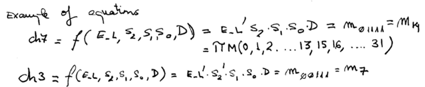 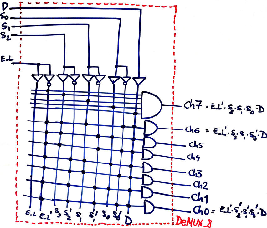 |
| Fig. 4. DeMUX_8 canonical equations and circuit representation. |
If you like to check the equations that you have inferred simply inspecting the truth table, you can run Minilog using this DeMUX_8.tbl file containing the circuit's truth table.
 |
| Fig. 5. List of SoP and PoS equations from minilog. |
Now it is easy to translate this circuit in Fig 4 into a VHDL file DeMUX_8.vhd ready for synthesis using FPGA EDA tools.
Plan B Translate the schematic in Fig. 3 into VHDL (DeMUX_8.vhd file) and synthesise it for a given target chip using FPGA EDA tools such Quartus Prime.
Test
Let us use a VHDL testbench fixture to apply signals or stimulus and test how the circuit works.
 |
| Fig. 6. Testbench fixture for testing the designed entity. |
Use a VHDL testbench (DeMUX_8_tb.vhd file) in ModelSim to verify that the demultiplexer works as expected in Fig. 2.
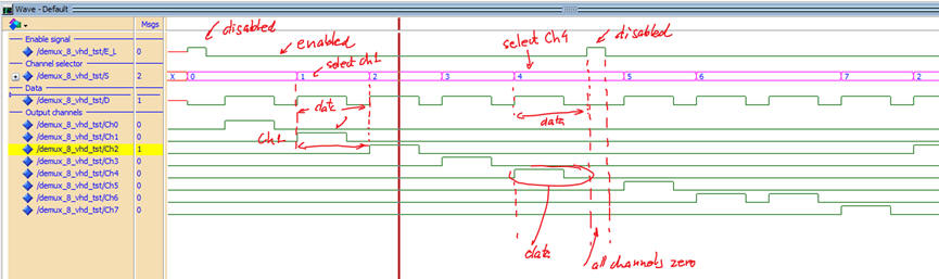 |
| Fig. 7. Timing diagram demonstrating how the circuit works. |
Or instead, capture the developed circuit based on logic gates in Fig. 4 in Proteus for a given classic technology (CMOS or LS-TTL) and run simulations.
1.7.3.3. DeMUX expansion circuits (plan C2)
For instance, how to invent a DeMUX_32 using small chips of the same kind?
- Draw the truth table of our DeMUX_32 symbol.
- Propose its internal architecture using DeMUX_8 components and other circuits if necessary.
1.7.3.4. Commercial chips
The chips 74HCT138 can operate as a demultiplexer.
- Draw the truth table of our DeMUX_8 symbol (Fig. 2).
- Study the chip's truth table from its datasheet.
- Propose its internal architecture using only the 74HCT138 chip and logic gates if necessary (plan C2).
- Capture and simulate your circuit in Proteus (method II) to demonstrate that it works as expected.
The chip 74HCT154 can be used as a demultiplexer.
- Draw the truth table of our DeMUX_16 symbol.
- Study the chip's truth table from its datasheet.
- Propose its internal architecture using only the 74HCT154 chip and logic gates if necessary (plan C2).
- Capture and simulate your circuit in Proteus (method II) to demonstrate that it works as expected.
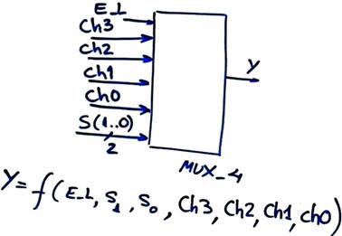
Activity #1: Plan A. Write the truth table of the MUX_4 symbol represented in Fig. 6. Find the following two equations and the corresponding logic circuits: (1) using ones and AND-OR-NOT-Buffer logic gates; (2) using zeros and only NOR2 gates. You can test your development using method II or method IV.
|
|
| Fig. 6. MUX_4 symbol. |
Activity #2: Play with the Proteus circuit MUX_DeMUX organised as a laboratory prototype.
Activity #3: Design the circuit DeMUX_16 from the previous lecture A #2 using either plan A or plan B and our set of VHDL tools for synthesis and simulation. Select as a target chip this MAX II EPM2210F324C3.
Remember that a project as a class activity requires this initial paper work:
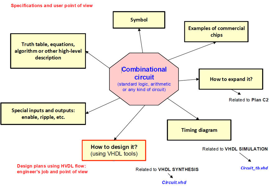
(1) Specs & theory (our map of concepts)
(2) Planning. How we solve design projects using VHDL tools? Which design strategy to translate into VHDL files? a) sketch (enough for exams and peer discussion) and b) totally annotated schematic required to start development.
This is the most important section of your project where you are going to explain using a flowchart concepts, ideas, proceedings, tools, schematics, equations, design steps or parts, locations, etc.
As usual, solve the project using handwriting and printing and commenting your computer results.
| Home Term 26/27-Q1 Contact Products Electronic devices and companies Software Books Magazines Instruments DEE Library EETAC DEEL |

|
|
| Web activa des de 09/2001, @ F. J. Robert, Web editat amb Microsoft Expression Web 4. El contingut és un complement als materials d'estudi del curs Circuits i Sistemes Digitals disponibles al campus digital Atenea. Llicència:Reconeixement 4.0 Internacional de Creative Commons |