|
|
Bachelor's Degree in Telecommunications Systems and in Network Engineering |
|
L2.1: Designing standard logic circuits using VHDL. Multiplexers [P2] Concept map associated to combinational circuits design. VHDL design flow |
[22 Sep] |
1.7. Standard combinational logic circuits
Once we have understood P1 basic ideas on Boole's algebra and circuit analysis and design using logic gates, let us continue presenting basic standard combinational blocks.
1.7.1. Concept map (for all standard circuits in P2, P3 and P4)
All combinational circuits (including arithmetic circuits in P3 and P4) are organised following this concept map in Fig. 1 and Fig. 2 rec.
1.7.1.1. Truth table, symbol, timing diagram
1.7.1.2. Chip expansion, enable input
1.7.1.3. Examples of commercial chips
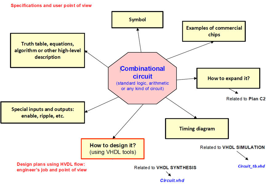 |
| Fig. 1. Concept map or mind map for organising circuit specifications. (Visio). All our combinational circuits will be observed from this frame. |
1.7.1.4. Plans or strategies to apply our VHDL design flow: plan A, plan B and plan C2
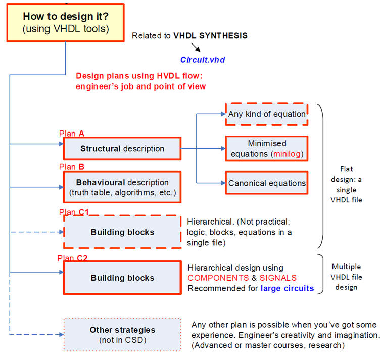 |
| Fig. 2. The three CSD strategies for planning circuits. Plan C1 is left only for designing FSM in P6. |
The concept map includes our VHDL design flow (Visio) for EDA tools that ends downloading the configuration file into the programmable chip. For instance, this Fig. 3 is a typical slide from the vendor Aldec.com that shows the concepts for designing circuits targeting FPGA chips.
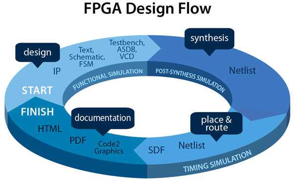 |
| Fig. 3. Typical commercial FPGA design flow sections. You see how the documentation section also becomes a fundamental part. |
1.7.2. Multiplexers or data selector
1.7.2.1. MUX_2, MUX_4, MUX_8, etc.
Specifications: Design a MUX_8
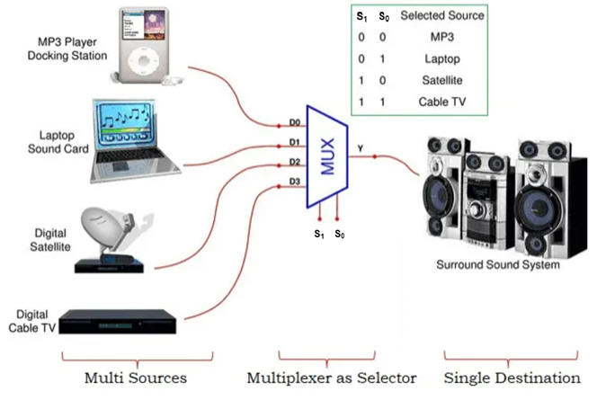
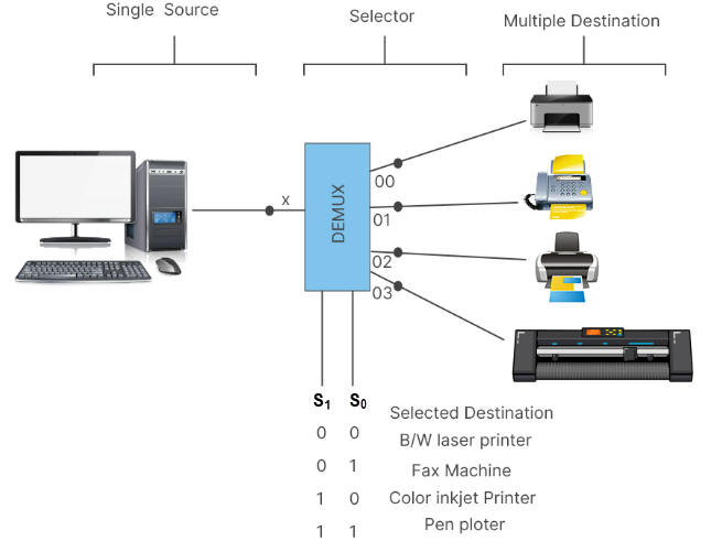
Theory and applications. What is a MUX or data selector? Play with this example of MUX_DeMUX.pdsprj simulation. The full prototype is at LAB2.
|
|
| Fig. 3. MUX-DeMUX application examples (source: ref.1, ref. 2). |
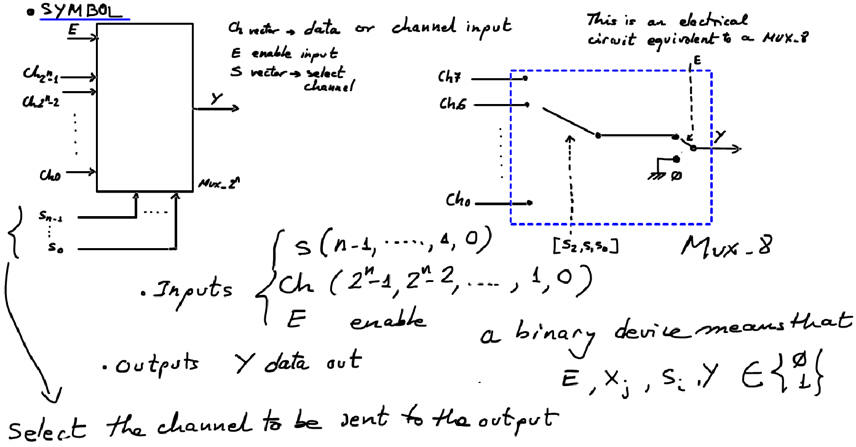
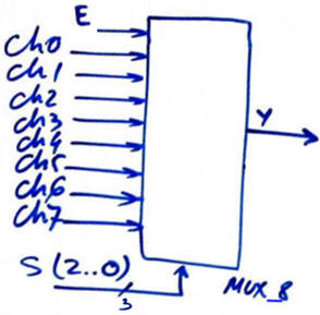
Symbol, truth table, special inputs, example of timing diagram, commercial circuits.
|
|
| Fig. 4. MUX_n circuit. |
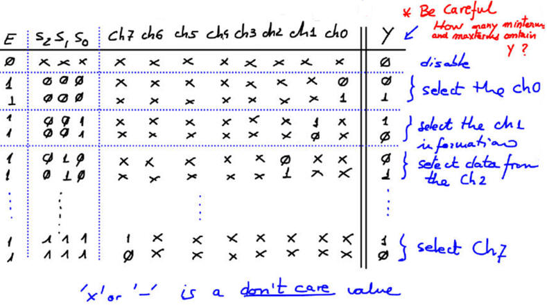
The symbol and truth table example for an 8-channel multiplexer (MUX_8) is represented in Fig. 5.
|
|
| Fig. 5. MUX_8 symbol and truth table. |
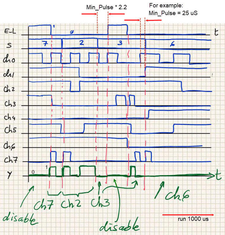
This timing diagram in Fig 6 is an example on how the signals evolve in time.
|
|
| Fig. 6. Timing diagram example. |
Full planning, development and testing is presented at LAB2 as design tutorials on plan A and plan B using our VHDL EDA tools (Minilog, Quartus Prime, ModelSim, etc.).
Plan A using equations and logic gates.
Is it possible to draw a canonical circuit based on product maxterms or sum of minterms?
|
|
Fig. 7. Discussion on whether is possible to infer canonical logic equations based on maxterms or minterms. |
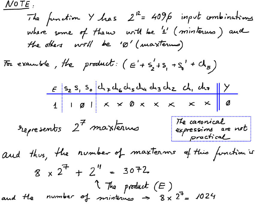
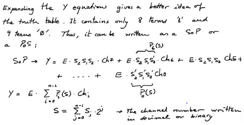
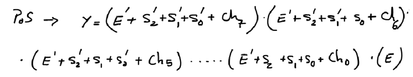
Thus, canonical circuits based on maxterms or minterms are not practical. We will try to find simpler equations like SoP or PoS. We have two alternatives: simplifying inspecting the truth table in Fig. 5 above, or minimising using minilog (as done in Lab2).
|
|
Fig. 8. Truth table simplified using all the '1' terms (products) and writing them as SoP. Equivalent logic circuit requiring 8 AND-5 gates and another OR-8 gates. |
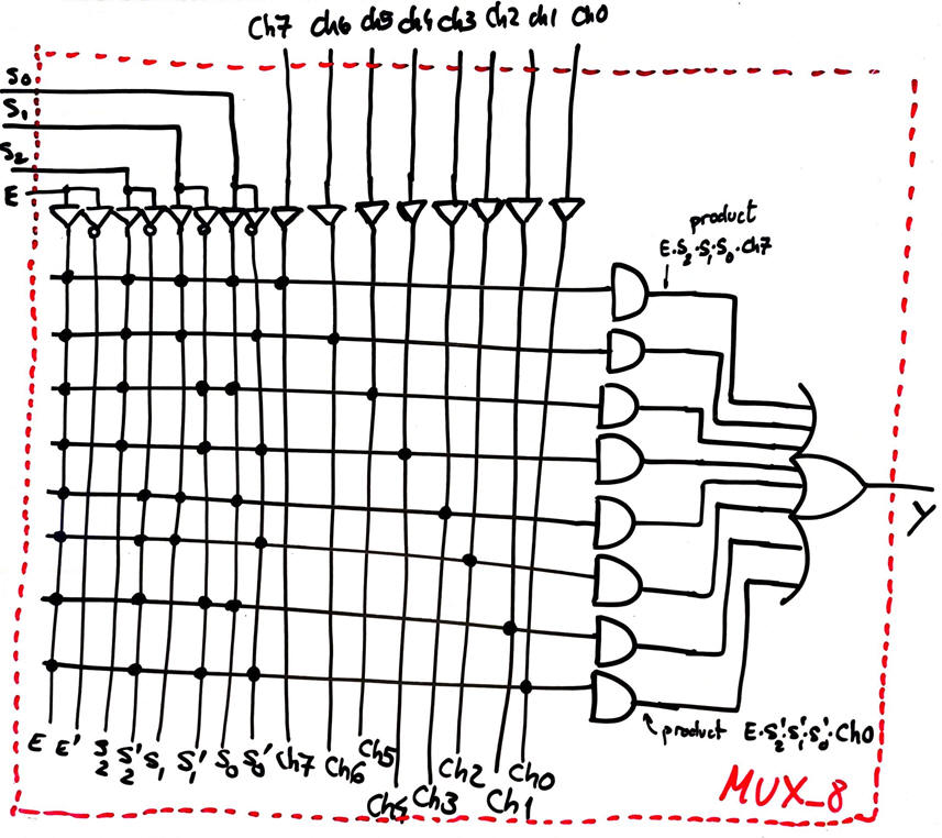
In the same way, we find a simplified equation inspecting the truth table and anding all the '0' terms (sums) in the form PoS, as shown in Fig. 9.
|
|
| Fig. 9. Equations and circuit using OR-5 gates (sums) and a final AND-9 (product) (PoS). Equivalent logic circuit. |
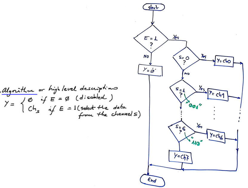
Plan B. Additionally and alternatively, we can "write the circuit", interpreting the truth table as an algorithm or flowchart that describes its functionality or behaviour.
|
|
Fig. 7. High-level definition of the MUX_8 truth table. |
1.7.2.3. MUX expansion circuits
Expanding circuits of the same kind is like applying our plan C2. For instance:
- How to build a MUX_16 using MUX_4 components?
- How to invent a MUX_8 using only MUX_2 components?
1.7.2.4. Commercial chips
74HCT151, 74HCT152, 74HCT153, etc.
Activity #1: Designing a DeMUX_4.
Specifications and theory: Draw the truth table of the DeMUX_4 represented in Fig. 1. Find a similar commercial chip. How long is the truth table? How many maxterms the circuit have? Write the minterms canonical equations. Explain any theory concept of your interest to explain the functionality and application of such standard circuit. Add a timing diagram and other concepts if necessary.
Plan: Draw a flowchart explaining the main concepts and procedures to design the circuit using VHDl tools and the strategy plan A based on minimised equations (SoP or PoS).
Project location: C:\CSD\P2\DeMUX_4\(files).
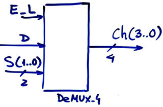 |
Fig. 1. DeMux_4 symbol. |
Development. Run Minilog and simplify using single output mode (SoM), equation output format, and choose PoS or SoP. Draw the logic circuit.
Test: Use Proteus or WolframAlpha (for instance, adapting a LAB1.1 tutorial) or VHDL tools (adapting LAB1.2 tutorial) to check the truth table of your circuit and discuss your project with your team mates.
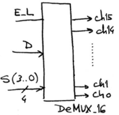
Activity #2: Complete the specifications section of the DeMUX_16 represented below drawing its truth table (and its canonical minterms equations), an example of timing diagram and finding an example of commercial chip. How long is the truth table? Find its equations.
|
|
| Fig. 10. DeMUX_16 symbol. |
| Home Term 26/27-Q1 Contact Products Electronic devices and companies Software Books Magazines Instruments DEE Library EETAC DEEL |

|
|
| Web activa des de 09/2001, @ F. J. Robert, Web editat amb Microsoft Expression Web 4. El contingut és un complement als materials d'estudi del curs Circuits i Sistemes Digitals disponibles al campus digital Atenea. Llicència:Reconeixement 4.0 Internacional de Creative Commons |