|
|
Bachelor's Degree in Telecommunications Systems and in Network Engineering |
|
Lecture 1 |
L6.1: Finite State Machine (FSM) [P6] The recipe for a systematical design of FSM. The first application: flip-flops conceived as FSM |
[6 Nov] |
2.5. Finite State Machine (FSM) architecture: a formidable conceptual idea. Therefore, let us apply it on all our projects chapter 2 and chapter 3 projects.
| FSM is the key for most of real-world applications |
|
- Motion control and any other subsystem - User interfaces, card readers, ... - Traffic control systems, highway access, pattern recognition - Self-driving cars and robotics - Media players and entertainment devices - Elevator control systems, washing machines, dishwashers, home appliances - Vending machines, ATM's, payment processing - HVAC (heating, ventilation and air conditioning) and climate control systems - Networking protocols, transmitters and receivers - and everything else you can imagine ... |
2.5.1.Specifications
2.5.1.1. Function table, symbol, state diagram (depending on the application it can be here in specifications or be the first concept in planning)
2.5.1.2. CLK and CD circuits
2.5.1.3. Example of timing diagram
2.5.1.4. Systematic design procedure (pdf). The sequence for designing FSM in our CSD course:
| CSD - P6: FSM design procedure |
|
1. Specifications a) Draw the project symbol and explain how the circuit works using function tables or similar descriptions. Propose the CLK oscillator and the asynchronous reset (CD) circuits. b) Draw a sketch of timing diagram because in this Chapter 2 representing the system evolving in time is a fundamental idea. Besides, it will be translated as an example stimulus process for testbenching. 2. Planning c) Infer a state diagram (sometimes it is discussed in specifications because it is a tool of great help to comprehend the project). Do it always in the same way: cycles, states; arrows, state transitions and loops; parenthesis in a different colour indicating outputs for each state. d) Draw the FSM general architecture.
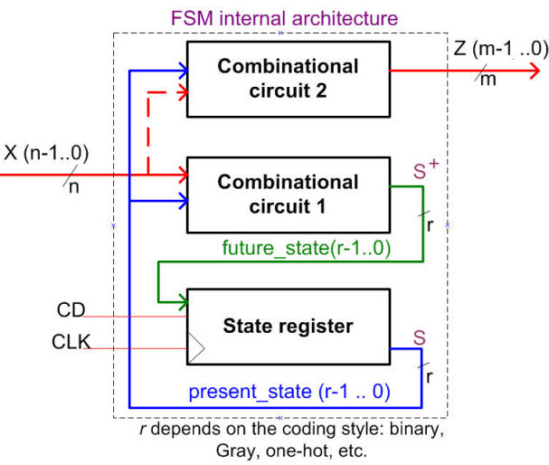
Fig. 1. FSM architecture in a single file (plan C1) using up to three processes. Signals future_state and present _state are also named next_state and current_state respectively. D_FF is the building block acting as state register (r-bit memory cell) to be used with combinational circuits form Chapter 1 to implement finite state machines (FSM). The present_state is updated after the CLK's rising edge. CD = '1' resets the FSM. e) Adapt the general FSM architecture to your problem and draw the state register based on a bank of D_FF. Deduce how many D_FF are required if you are coding states in binary sequential (radix-2), one-hot, Gray, Johnson, etc. f) Write the truth table of CC2 and its equivalent behavioural (plan B) interpretation as a flowchart. CC2 is for calculating outputs, thus, this combinational circuit implements all the signals drawn in parenthesis in the state diagram. g) Write the truth table of CC1 and its equivalent behavioural (plan B) interpretation as a flowchart. CC1 is for calculating the next state to go, thus, this combinational circuit is in charge of all the circuit state transitions (arrows). 3. Development h) Write the VHDL file (plan C1, a single file containing three processes representing the translation of the FSM. State-type signals: state enumeration. Find an example to copy and adapt. i) Run a project using an EDA synthesis tool for a CPLD or FPGA target chip. j) Discuss RTL and technology schematics. Check the number of registers D_FF used, which will depend on the state encoding. 4. Test (functional) k) Generate the skeleton of the testbench fixture. Translate your initial timing diagram sketch into VHDL stimulus processes. Consider the parameter TCLK as the CLK_period constant and how long the simulation has to run. Write the the CLK signal in a separated process. l) Simulate the circuit using your VHDL testbench and discuss your results. Represent as well the waveforms of the current_state and next_state signals in wave diagrams. 5. Test (gate-level) m) Simulate the technology circuit (flat vho, sdo or sdf) using your VHDL testbench and discuss results. Measure propagation delays in a given signal transition from CLK to output (tCO). n) Using the timing analyser tool, measure the worst propagation delay and deduce the CLK's maximum frequency of operation that can be applied to your FSM design considering a given target chip. 6. Prototyping (planning and synthesising a new top entity) o) It is always possible to use any of our lab training boards for CPLD or FPGA to synthesise the circuit, for instance the DE10-Lite. See how many additional circuits are required for the adaptation (CLK_Generator, 7-segment decoders, etc. Design your plan for the new top entity. p) Assign your top entity inputs and output pins using the pin assignment spreadsheet or the pin editor tool. q) Generate the sof and pof FPGA configuration files ready for downloading. r) Use the programmer app and experiment in the lab using real instrumentations for measurements and characterisation. 7. Report (handwritten) and presentation s) Follow usual indications on how to report and present your materials. It is easy for most circuits to generate more that twelve pictures, sketches, diagrams, computer results, etc. to report perfectly well how the circuit that you have invented is conceived and how does it perform. Report pictures may be used later as slides for oral presentations and recordings. |
Ref: General ideas on designing FSM (Advanced Micro Devices AMD, 1993).
2.5.2.Planning
2.5.2.1. Architecture: canonical, synchronous, plan C1: hierarchical, structural in a single VHDL file
Let us introduce the key concept and architecture of finite state machine (FSM) as the standard canonical synchronous sequential system to solve most of applications. In CSD we represent the FSM as a hierarchical three block (or processes) structure in a single VHDL file: plan C1. The only time in CSD where this plan is used.
2.5.2.2. State diagram, and FSM adaptation
2.5.2.3. State register: r-bit memory (D_FF), state encoding (binary sequential, Gray, one-hot, etc.)
2.5.2.4. Output logic (CC2): truth table, behavioural interpretation: flowchart
2.5.2.5. Next state logic (CC1): truth table, behavioural interpretation: flowchart
2.5.3. Developing
2.5.3.1. VHDL translation, state enumeration, project location.
2.5.3.2. Synthesis project for a target chip. FSM encoding options
2.5.3.3. Target chip resource usage (D_FF registers)
2.5.3.4. RTL and technology view discussion
2.5.3.5. FSM state diagram discussion
2.5.4. Testing (functional)
2.5.4.1. Test-bench fixture schematic and test-bench VHDL file
2.5.4.2. CLK and other signals stimulus processes
2.5.4.3. Functional simulation and wave results discussion
2.5.4.3. Internal signals representation (current_state, next_state)
2.5.5. Testing (technology)
2.5.5.1. Gate-level (timing) simulation and results discussion
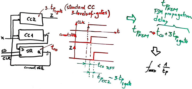
2.5.5.2. Propagation time CLK to output measurements for the state register flip-flops (tCO). How does a circuit behave in a given active CLK transition?
2.5.5.3. Timing analyser spreadsheet and measurement of the maximum frequency of operation. What is the worst longest propagation delay for a given synchronous circuit such the FSM? Discuss in which way D_FF set-up and hold time may affect the assumptions below.
2.5.6. Prototyping
Our applications can be put into practice using FPGA training boards. Example of prototyping are given in LAB6 and LAB7 tutorials.
2.6. Examples of FSM in VHDL: single-file (plan C1) projects
2.6.1. Designing flip-flops as FSM (two-state machines)
We have developed full tutorials on designing basic flip-flops as FSM in VHDL. You can use these materials for both, comprehending how flip-flops work, and also as introductory examples to FSM design because they contain only two states.
2.6.1.1. RS flip-flop (RS_FF is JK_FF never using J = 1; K = 1}
2.6.1.2. D-type (data) flip-flop {D_FF}
2.6.1.3. JK flip-flop {JK_FF}
2.6.1.4. T-type (toggle) flip-flop {T_FF}
And now, once considered these simple two-state systems, we can continue examining any other example of FSM application. For instance, before attempting the next class on a 16-key matrix keypad, we can get an idea on a bicycle flashing lamp with a single push-button or LAB6 on classroom luminaries.
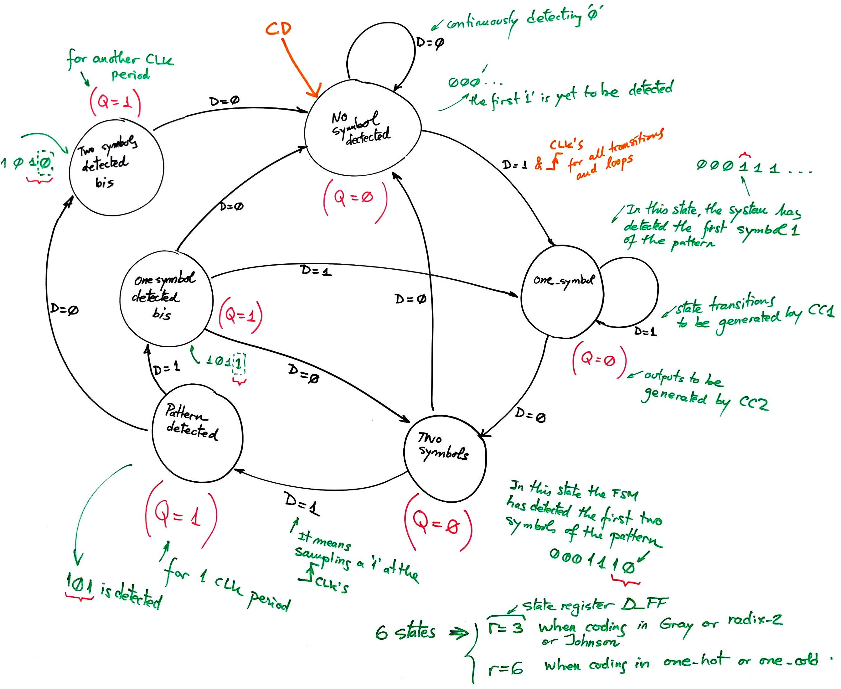
Activity #1: Solve this sequence detector that works sampling continuously a bit stream of data.

Draw a state diagram to run this application. Imagine states labels such: "No_symbols", "One_symbol", etc. No_symbols is the initial state of the FSM where none of three symbols of the pattern has been sampled yet.
Find and study a similar circuit, for example from Chapter 2 product assignments.
Additional question: How to modify the state diagram if we impose that the output pulse Q has to be of a duration TQ = 2·TCLK?. This is an idea, check it drawing another timing diagram representing also the internal states.
Optional as class activity (only if you have study time available to spare on it). Design and test the full circuit following our FSM procedure. NOTE that you can not develop unless all the diagrams and tables from sections c, d, e, f, g are completed. Draw your testbench schematic (section k) before testing your circuit functionally.
Activity #2: Draw the timing diagram and propose an state diagram for this bicycle lamp torch:
 |
Specifications. Commercial torch. Only one push button PB to control operations. First click: do nothing (as if the button were clicked accidentally). In a second design phase this feature can be added: after 2 min. of waiting for another click, it goes back to the initial state. Second click: light ON. Third click: Blinking lamp at 5 Hz. Fourth click: light OFF. |

Planning. Let us proposed the following hardware. The CLK_generator will be covered in L8.2.

We can also sketch in time how the lamp Z will work when the user clicks the PB several times. Let us propose an accurate timing diagram for the FSM Chip1 imagining as well what states we may introduce to identify each event.
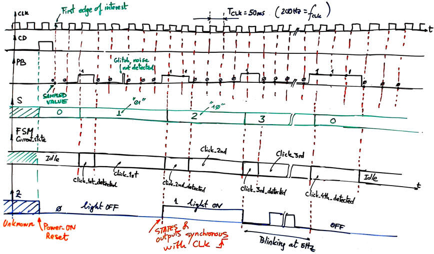
Let us propose the FSM state diagram once we can see how the PB will be sampled cyclically at the CLK's rising edge. We always will represent output values at each state in red coloured brackets.

And from now on, the project can be solved automatically following our systematic VHDL procedure to synthesise the circuit (RTL and technology views). We will continue testing the circuit (functionally and at the gate-level) using a convenient testbench to drive both, CLK periodic waveform and CD and PB pulses.
The full design, the complete sequence of steps on how we apply the FSM recipe is similar to this tutorial application: Torch flashing light.
This picture from ModelSim shows how the system works.

You are also invited to implement the project as a prototype for the DE10-Lite board.
This is the full project Torch_driver.zip adapted to the legacy board Coolrunner-II from Xilinx (AMD).
| Home Term 26/27-Q1 Contact Products Electronic devices and companies Software Books Magazines Instruments DEE Library EETAC DEEL |

|
|
| Web activa des de 09/2001, @ F. J. Robert, Web editat amb Microsoft Expression Web 4. El contingut és un complement als materials d'estudi del curs Circuits i Sistemes Digitals disponibles al campus digital Atenea. Llicència:Reconeixement 4.0 Internacional de Creative Commons |