|
|
Bachelor's Degree in Telecommunications Systems and in Network Engineering |
|
Lecture 3 |
L2.3: Designing standard logic circuits. VHDL: Decoders and encoders [P2] Flat (single VHDL file) plans: structural plan A / behavioural plan B |
[25 Sep] |
1.7.4. Binary decoder
1.7.4.1. Dec_3_8, Dec_4_16
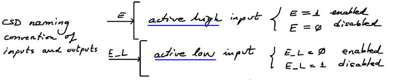
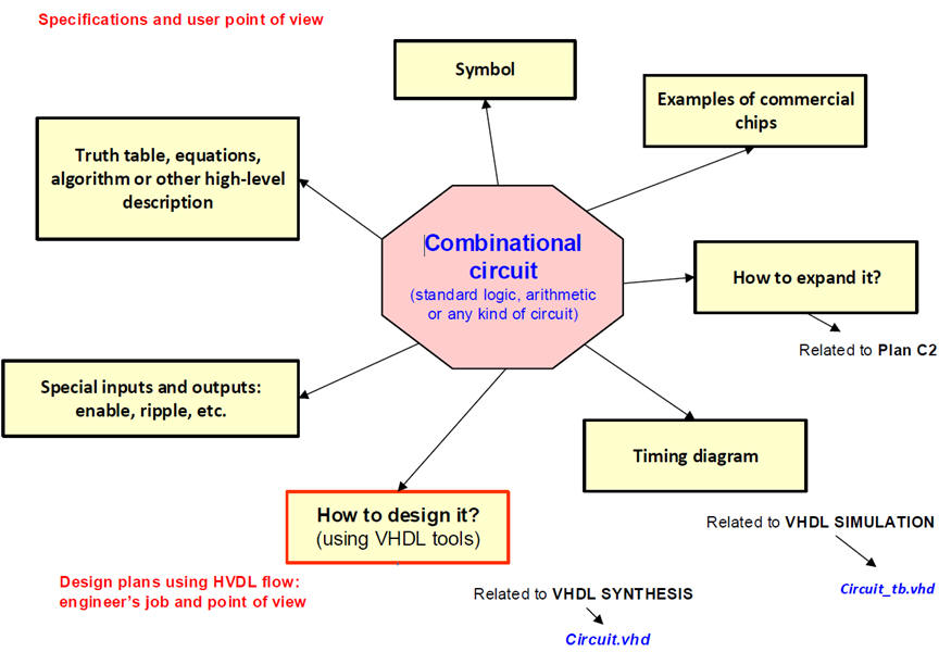
Discussing binary decoder basics and specifications rec.. From our concept map: 1) Symbol, (2) truth table or equations, (3) timing diagram, (4) commercial chip, (5) internal design (Plan A, B, C1 or C2), (6) how to expand them (Plan C2 in P3)?
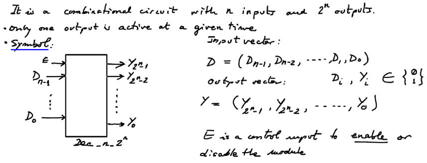  |
| Fig. 1. Generic binary decoder symbol. |
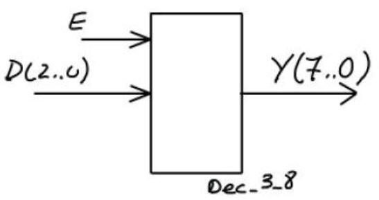
Fig. 2 shown the symbol and truth table when n = 3, it is a Dec_3_8 device.
 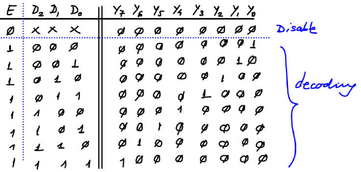 |
| Fig. 2. Dec_3_8 truth table. |
1.7.4.2. Design examples
- Plan A. This tutorial is the complete design using VHDL tools of the decoder Dec_3_8 using equations.
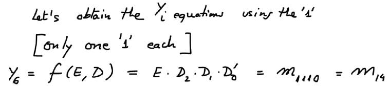   |
| Fig. 3. Structural equations inferred inspecting the truth table. |
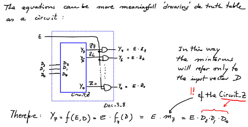
Finally, we can draw this eight equations based on canonical minterms as represented in Fig. 4.
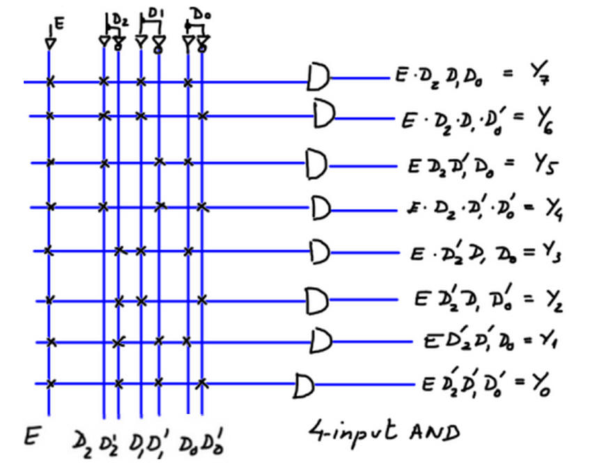 |
| Fig. 4. Circuit based on minterms. |
- Plan B. This tutorial is the complete design using VHDL tools of the decoder Dec_3_8 using the truth table, algorithm flowchart or any other high-level interpretation.
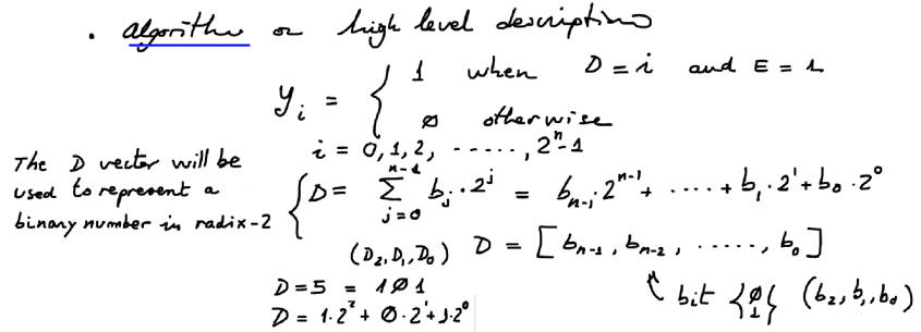 |
| Fig. 5. Circuit algorithm. |
1.7.4.3. Decoder expansion circuits (plan C2)
1.7.4.4. Commercial chips
74HCT138, etc.
1.7.5. Binary encoders (priority high)
1.7.5.1. Enc_8_3, Enc_10_4
The symbol for an Enc_8_3 is represented in Fig. 6 and its truth table in Fig. 7.
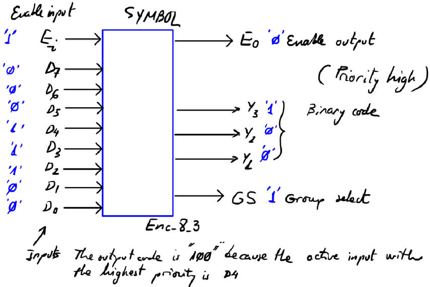 |
| Fig. 6. Circuit Enc_8_3. |
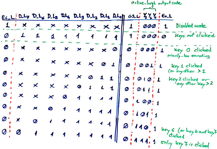
This truth table is 512 rows long. It can be written in a compact form using don't care terms as shown in Fig. 7.
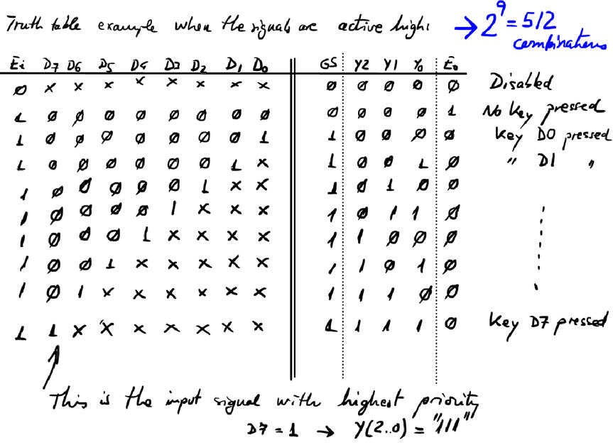 |
| Fig. 7. Enc_8_3 truth table. |
And an example of timing diagram is represented in Fig. 8.
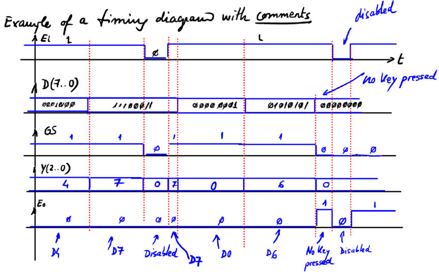 |
| Fig. 8. Enc_8_3 timing diagram example. |
We can start thinking now on design plans, for instance Plan A trying to deduce some equations.
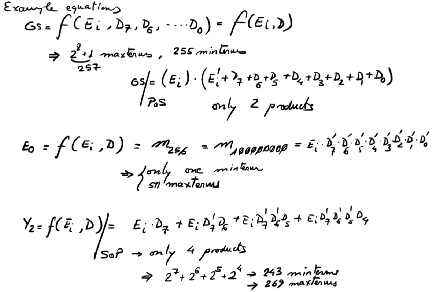 |
| Fig. 9. Some equations after exploring the truth table. Using Minilog will generate the complete list of output functions in SoP or PoS form, ready for VHDL translation as Enc_8_3.vhd source file. |
1.7.5.2. Design examples
- Plan A. Discussion of the binary encoder Enc_10_4 using equations.
- Plan B. Discussion of the binary encoder Enc_10_4 using the truth table, algorithm or any other high-level interpretation.
1.7.5.3. Encoder expansion circuits (plan C2)
1.7.5.4. Commercial chips
74LS148, 74LS147, CMOS 4532B, etc.
Activity #1: Invent an Enc_8_3 with priority-low using our VHDL tools adapting the symbol and its truth table from the commercial circuit 74LS148.
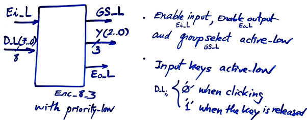
Priority-low means that when clicking several keys at the same time, the circuit generates the binary radix-2 code corresponding to the lowest number. For instance, if you click simultaneously keys 7, 5 and 2, the encoded output is "010".
Use one of these plans:
- Plan A equations. Use Minilog to obtain SoP or PoS.
Project location: C:\CSD\P2\Enc_8_3\PlanA\(files)
- Plan B high-level description. Draw a flowchart or an schematic to translate the circuit's truth table into VHDL.
Project location: C:\CSD\P2\Enc_8_3\PlanB\(files)
Remember that a project as a class activity requires this initial paper work:
(1) Specs & theory (our map of concepts)
(2) Planning. How we solve design projects using VHDL tools? Which design strategy to translate into VHDL files? a) sketch (enough for exams and peer discussion) and b) totally annotated schematic required to start development
Activity #2: Adapt, using logic gates if necessary, the 74HCT138 commercial chip to the symbol in picture Fig. 2.
This activity is for learning subcircuits in Proteus.
Activity #3: Fig. 1 shows the symbol and the truth table of an 8-to-3 encoder (Enc_8_3). When several inputs are active high at the same time, a binary code is generated of the highest priority signal. The symbol "-" means a "don't care" value that is represented other times by "x". GS goes high when any input is assessed, thus it can be used both as a flag to indicate that a key is pressed and for disambiguation of the code "000". Design the circuit using plan C2 and Enc_4_2 components. Study and adapt materials from this similar project Enc_10_4 using Enc_8_3.
 |
|
Fig. 1. The symbol and truth table of an Enc_8_3. |
| Home Term 26/27-Q1 Contact Products Electronic devices and companies Software Books Magazines Instruments DEE Library EETAC DEEL |

|
|
| Web activa des de 09/2001, @ F. J. Robert, Web editat amb Microsoft Expression Web 4. El contingut és un complement als materials d'estudi del curs Circuits i Sistemes Digitals disponibles al campus digital Atenea. Llicència:Reconeixement 4.0 Internacional de Creative Commons |