|
|
Bachelor's Degree in Telecommunications Systems and in Network Engineering |
|
Laboratory |
Laboratory 10: FSM in C language. Interrupts to detect signal events (CLK) [P10] FSM: state enumeration (plan X) FSM: arithmetic operations (Plan Y) |
[3 Dec] |
This is the post lab assignment PLA10_11. |
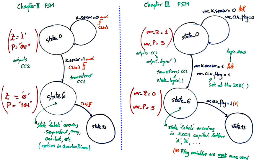
This laboratory session will show you how to use interrupts to detect external events such signal transitions and thus implement FSM as we did in Chapter II. External events detected by means of interrupts (INT0, INT1 or IINT2) such CLK edges will allow us to adapt and rebuild using µC most of our circuits.
Furthermore, the proposed examples in this lab are counters, to be able to discuss both, plan X: typical FSM from P6 enumerating states, and plan Y for large counters using arithmetic operations.
The adaptation means drawing the FSM state diagram using RAM variables. This slide shown the comparison.
3.5.4. Examples
3.5.4.3. Counter_BCD_1digit: 1-digit BCD up counter (plan X)
Project tutorial #1: Counter_BCD_1digit |
We will prototype and characterise the FSM using our platform CSD_PICstick , the MPLAB SNAP programmer and the the VB8012 compact instrument. LAB10 control sheet.
3.5.4.4. Counter_mod1572 (large binary counter plan Y)
Project tutorial #2: Counter_mod1572 |
| Home Term 26/27-Q1 Contact Products Electronic devices and companies Software Books Magazines Instruments DEE Library EETAC DEEL |

|
|
| Web activa des de 09/2001, @ F. J. Robert, Web editat amb Microsoft Expression Web 4. El contingut és un complement als materials d'estudi del curs Circuits i Sistemes Digitals disponibles al campus digital Atenea. Llicència:Reconeixement 4.0 Internacional de Creative Commons |