|
|
Bachelor's Degree in Telecommunications Systems and in Network Engineering |
|
Chapter II: Sequential systems. L5.1: Basic idea of memory and the cell RS latch [P5] 1-bit asynchronous memory cell: RS latch |
[16 Oct] |
2.1. The concept of memory in digital circuits
The concept of internal state (current/present state and next/future state)
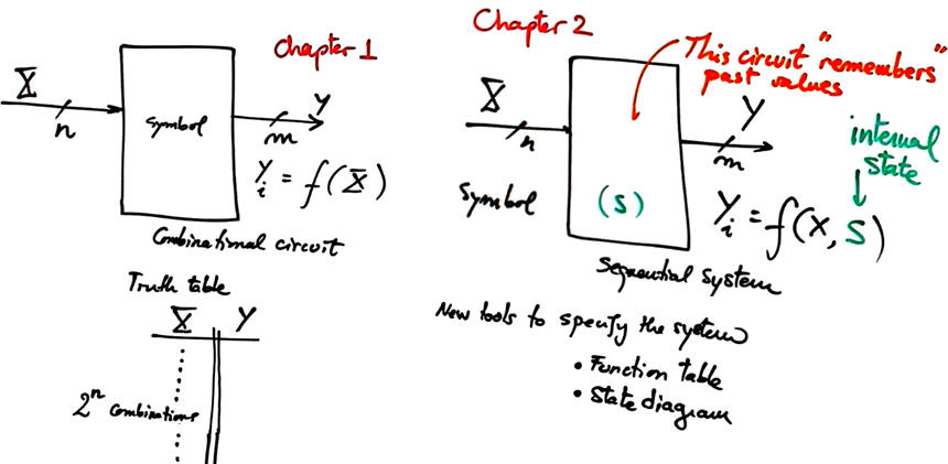 |
Fig. 1. What is a sequential system? Why it is different from a combinational circuit? What is an internal state? How is memory implemented in a circuit? What is current/present state and future/next state? When is present and when is future? |
Those are difficult questions to answer at this point in the course; truth tables are not valid anymore for specifying circuits in this new chapter 2. Therefore, as usual we better comprehend such questions step by step and using simple examples and applications.
2.2. Latch circuits: asynchronous 1-bit memory cells
2.2.1 Latch RS (RS_latch).
2.2.1.1. Function table, state diagram, timing diagram
1. Specifications
The Set-Reset latch (RS_latch) is the simplest 1-bit memory cell. The aim of this tutorial is to deduce it using logic gates, how to translate the schematic into VHDL and how to simulate it using a VHDL testbench, therefore its function table can be verified rec.
This is the simplest device intended to save a '1' or a '0' using the control inputs set (S) and reset (R). The output Q is kept/stored/written/saved/maintained/memorised forever unless a new input order changes its value. Naturally, at power on time the cell's output is unknown, thus an initial reset or preset is required to start operations.
And, due to the definition of the control inputs, it is unpredictable what may happen to the output when both signals and activated at the same time.
The entry from Wikipedia: RS latch cell.
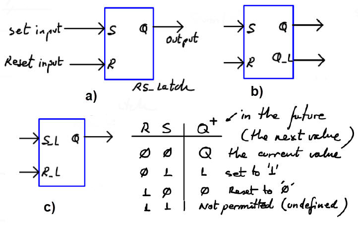 |
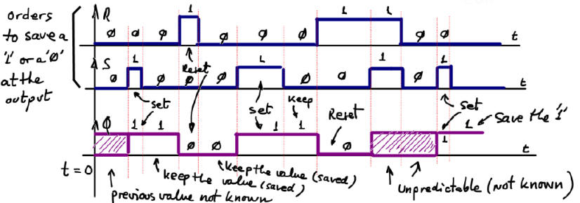
Fig. 2. Symbols, function table and example timing diagram of a RS latch (RS_latch). Preferably the symbol a) active-high will be used. It is highly recommendable to annotate comments on waveforms and tables to fully comprehend how sequential circuit will work. |
 |
|
2.2.1. 2. How to design RS_latch using gates (structural plan A from Chapter 1)
At this point in the course, the first question to ask is: How to build an RS_Latch from logic gates, thus climbing another step from Chapter 1 (logic gates ---> RS_latch)?. Can we go to the lab and test our RS_latch circuit? Can we develop it using VHDL?
2. Planning
In Fig. 3 there is the circuit's state diagram. It is the best tool to describe how it works complementing the function table and the timing diagram. And it is going to give us an idea on how to derive a circuit based on gates for this memory cell. rec.
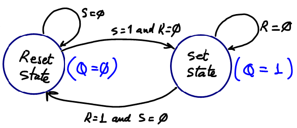 |
Fig. 3. State diagram where the arrows indicate the transitions between states accordingly to the given condition. And in parenthesis, in each state there is the annotation of the output values. To make it easy, different colours are used to represent outputs and state transitions. |
Why this circuit is not combinational? If we imagine that such circuit can be like the ones described in the previous chapter 1, we have the problem represented in Fig.4: a simple truth table cannot fully represent the functionally of this circuit, an input combination cannot have two different outputs.
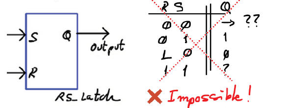 |
Fig. 4. Using a truth table is impossible to solve the idea of "memory". Which is the expected output for an input combination such as S = 0, R = 0 ? The answer is that both outputs are possible, therefore, this system cannot be combinational. We have to invent something else. |
Let's start thinking, as represented in Fig. 5 how a circuit idea can help to solve this 1-bit memory cell. How to deduce the RS_latch using logic gates? The key idea: if what we have to remember is the output Q, why not wire it back as an input?
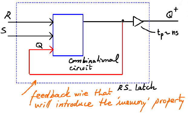 |
Fig. 5. The idea of a feedback wire to "remember" the current state makes the circuit feasible because the truth table is larger now and give us more options. Q+ represents the idea of the output a few ns later. The future or next value of the output Q will be a function of its current value and the inputs: Q+ = f(R, S, Q) |
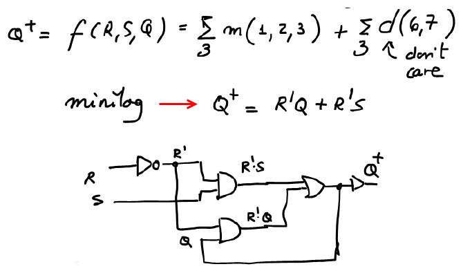
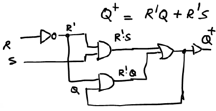
Solving the truth table represented in Fig. 6a, by means of canonical logic equations (minterms) and simplifying them as a SoP, a circuit is obtained.
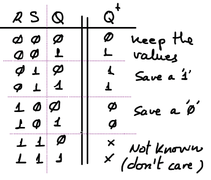 |
Fig. 6a. The truth table of the circuit now has 3 inputs, giving us a chance to solve the memory property of saving current outputs values when inputs are not active.
|
 |
|
Fig. 6b. Canonical equation and the equivalent circuit after having used Minilog.exe RS_latch.tbl to simplify the canonical expression to obtain a SoP equations RS_latch_corrected.txt. |
Further on, we can use for instance only-NOR (or only-NAND gates to visualise the most famous implementations of the RS latch cell already seen in commercial chips:
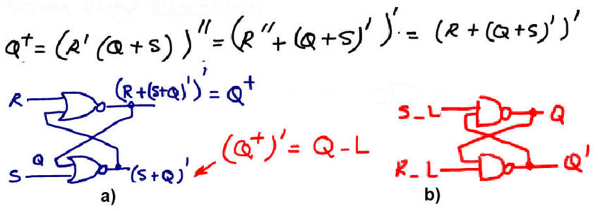 |
| Fig. 7. a) Only-NOR typical circuit, which also produces the complementary output Q_L = Q' . b) Only-NAND circuit which has the same functionality but using active-low inputs. |
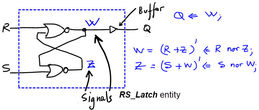
3. Development
This is the structural RS_latch.vhd circuit translating Fig. 7 equations above to VHDL, so that the EDA synthesiser generated exactly the expected circuit as shown in Fig. 7 rec.
 |
|
Fig. 8. The VHDL description of the circuit based on only-NOR gates ready for synthesis using EDA tools. |
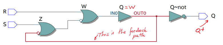
The RTL view schematics produced by the synthesiser copied in Fig. 9 is similar to our proposed circuit, but Quartus Prime has modified the equations.
 |
|
Fig. 9. The RTL view produced by the EDA synthesiser. |
The technology view schematics produced by the synthesiser when targeting a MAX II device.
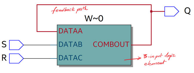 |
| Fig. 10. The technology view shows how only one logic element is used for implementing the RS_Latch. |
4. Testing (functional)
This is a sample VHDL testbench RS_latch_tb.vhd that is a translation of the timing diagram above in the specifications in Fig. 2. The testbench fixture is represented in Fig. 11 as usual.
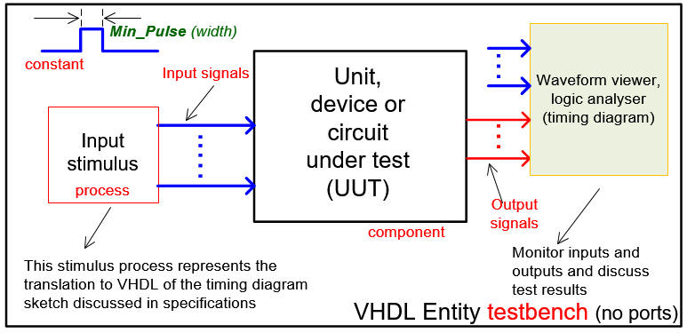 |
| Fig. 11. Testbench VHDL schematic. |
Run the EDA VHDL tool and demonstrate how the circuit works adding handwriting comments to the printed sheet of paper containing the waveforms.
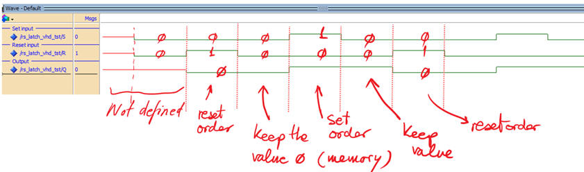 |
| Fig. 12. Example of a timing diagram to show how the circuit works. |
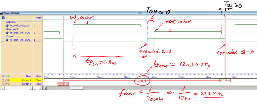
5. Testing (gate-level)
Gate-level simulation to calculate input-output propagation times and circuit speed for a given target PLD (Intel MAX II). Fig. 13 represents both transitions, showing that propagation delays tPHL = 5.27 ns and tPLH = 5.49 ns are similar but not identical.
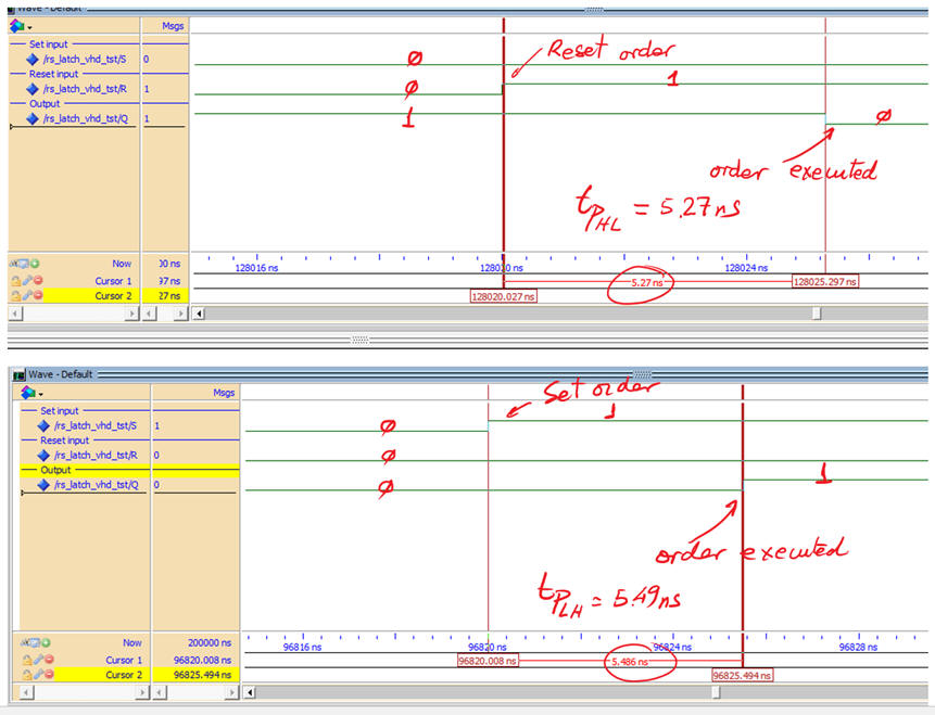 |
| Fig. 13. Measuring gate delays in output transitions. |
If we like to measure how fast can be this circuit switching output Q, we can infer the dynamic experiment in Fig. 14. R and S stimulus will be easily translated to VHDL.
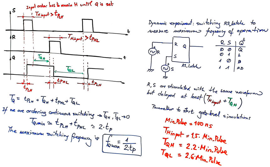 |
| Fig. 14. Stimulating the LS_Latch at ns propagation time scale. |
Results near the maximum switching frequency when applying this stimulus file RS_latch_tb.vhd.
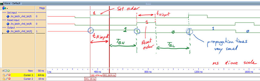  |
| Fig. 15. Stimulating the RS_Latch at ns propagation time scale (TQH = TQL = 0.3·Min_Pulse. |
2.2.1.3. RS_latch used as push-button debouncing circuit
An alternative simulation. This is the RS_latch.pdsprj running in the Proteus virtual laboratory. Here you can see as well how the circuit has an immediate application to solve the electrical signals bouncing associated to mechanical switches and push-buttons.
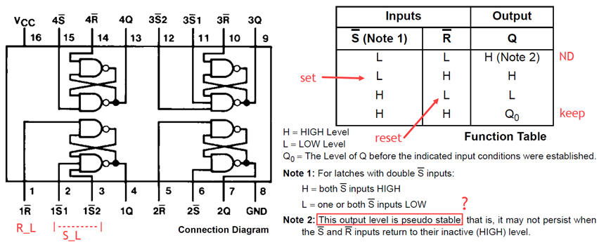
2.2.1.4. Commercial circuit
This is a commercial quadruple RS latch 74LS279. Each manufacturer uses its own naming styles and conventions, this is why we adapt these chips to our own CSD styles and symbols.
2.2.2. Transparent D latch (D_latch)
2.2.2.1. Function table, state diagram, timing diagram
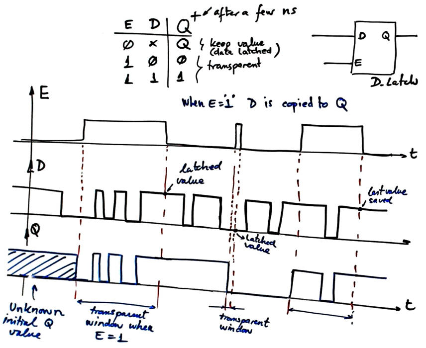
How to design it using gates using the same RS_latch approach?
What kind of applications may require such memory cell?
2.2.2.2. Commercial circuit
This is a commercial dual gated D latch 74HCT75 (data latch, also called transparent latch) to better grasp the meaning of enable input in this context of memory cells. What is the difference between an enable input and a CLK input?
Activity #1: How fast is this RS_latch circuit implementation? The logic gates are from classic CMOS technology. Find the reference of a similar latch integrated circuit in CMOS technology.
| Home Term 26/27-Q1 Contact Products Electronic devices and companies Software Books Magazines Instruments DEE Library EETAC DEEL |

|
|
| Web activa des de 09/2001, @ F. J. Robert, Web editat amb Microsoft Expression Web 4. El contingut és un complement als materials d'estudi del curs Circuits i Sistemes Digitals disponibles al campus digital Atenea. Llicència:Reconeixement 4.0 Internacional de Creative Commons |