|
|
Bachelor's Degree in Telecommunications Systems and in Network Engineering |
|
Laboratory |
Laboratory 9: microcontrollers. Basic digital I/O. Software organisation [P9] IDE and µC tools: C language, break points, step by step mode, watch windows, etc. |
[26 Nov] |
This is the post lab assignment PLA9. |
3.4. Digital I/O. Combinational circuits in C for learning how to organise simple programs and basic I/O
3.4.1. Specifications
3.4.1.1. Truth table, symbol, timing diagram
3.4.1.2. Symbol
3.4.1.3. Timing diagram
Project tutorial: Dual_MUX_4 using microcontroller and C |
EDA software resources:
| Chapter 3 |
| PROTEUS VSM(9.0 SP6) Notepad++ |
| C language |
| IDE tools for microcontrollers: Microchip (PIC18F/16F/ATmega) MPLABX (v6.25) / XC8 (v. 3.00) |
| Digilent WaveForms CSD_PICstick |
Learning how to develop and test interactively microcontroller projects
|
Key indications for saving study
time and learning these materials correctly:
Step-by-step tactical approach for developing and testing the project:
Read one input at a time and run simulations to watch that the voltage
value is correctly digitalised as a valid value in
RAM memory. In the same fashion, write one output at a time
and run to check that your code is correct to light a LED
connected at the assigned output pin. Solve the truth
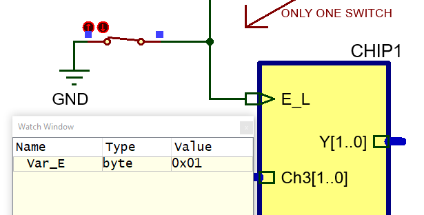
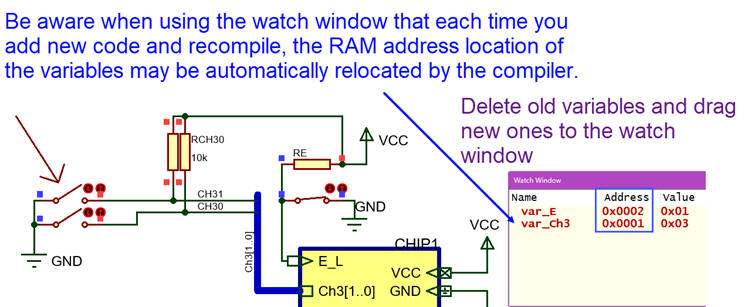
table algorithm and run t watch RAM variables. The three functions are totally independent and the order in which they are coded is not important. Or alternatively, the development and testing of the three functions can be assigned to three students working in the same cooperative group. Reading inputs Step #1): Hardware. Consider the circuit with oscillator, reset, and only the pin E_L connected to pin RC3.This is the file "Dual_MUX_4.pdsprj". Save it at the working directory. Software. Comment or delete all the code that is not referred to E_L. Translate the Fig 9 flowchart into C code. This is the file "Dual_MUX_4.c". Include as well "config.h" in your project. Save it at the working directory. Start a new project for a PIC18F46K22 and compile. Run simulations and add the watch window to monitor the RAM value var_E.
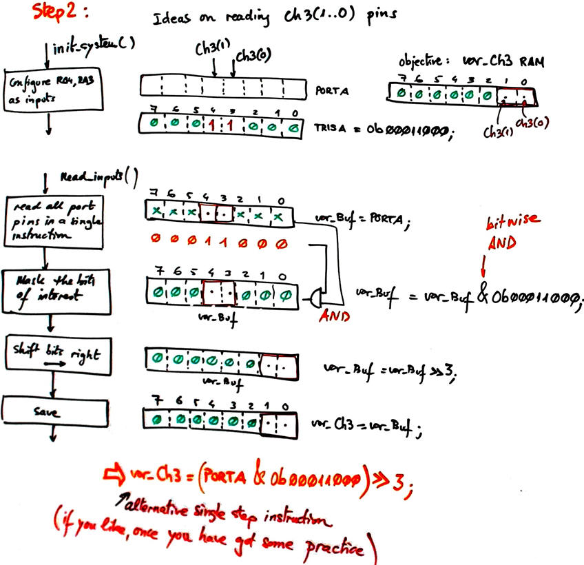
Step #2): Hardware. Add a new input in the schematic, for instance Ch3(1..0) "Dual_MUX_4.pdsprj". Software. Translate to C the planned flowchart and add it to the previous program "Dual_MUX_4.c".
Repeat new steps to complete all inputs. |
||||
|
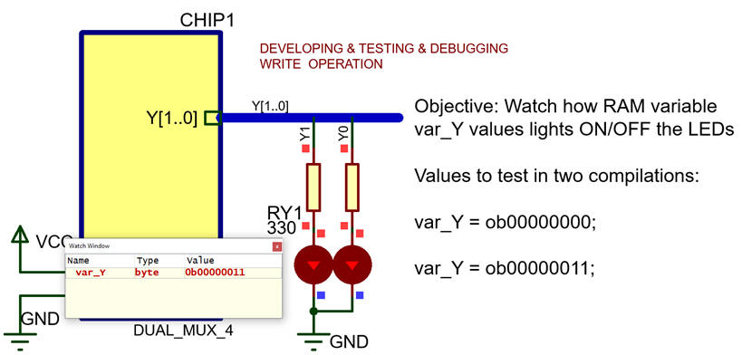
Writing outputs #1): Hardware. Add a pair of LED to visualise Y(1..0). This is the file "Dual_MUX_4.pdsprj". Save it at the working directory.Software. Comment or delete all the code that is not referred to var_Y. Translate the Fig. 10 flowchart into C code. This is the file "Dual_MUX_4.c". Save it at the working directory. Start a new project for a PIC18F46K22 and compile. Run and add the watch window to monitor the RAM value var_Y when at the same time you check that the LED are lighting correctly.
Add similar writing steps in projects with more outputs. |
||||
|
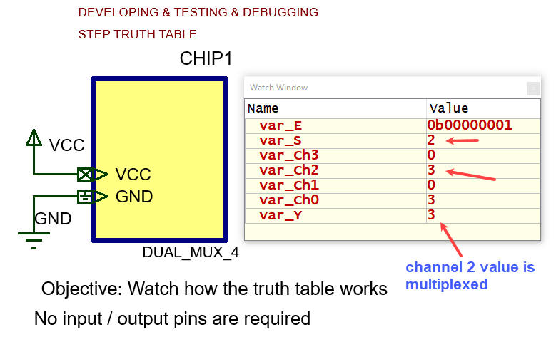
Truth table Hardware. Consider the circuit only with oscillator and reset. This is the file "Dual_MUX_4.pdsprj". Save it at the working directory.Software. Variables read as outputs from read_inputs() function will be simulated by fixed values in successive compilations. Translate the Fig. 11 flowchart into C code. This is the file "Dual_MUX_4.c". Save it at the working directory. Start a new project for a PIC18F46K22 and compile. Run and add the watch window to monitor the RAM values related to the truth table execution. Try other variable values recompiling the code.
|
Example video rec to show initial steps on how to start a new project in MPLABX for target PIC18F, compile and simulate
| Home Term 26/27-Q1 Contact Products Electronic devices and companies Software Books Magazines Instruments DEE Library EETAC DEEL |

|
|
| Web activa des de 09/2001, @ F. J. Robert, Web editat amb Microsoft Expression Web 4. El contingut és un complement als materials d'estudi del curs Circuits i Sistemes Digitals disponibles al campus digital Atenea. Llicència:Reconeixement 4.0 Internacional de Creative Commons |