|
|
Bachelor's Degree in Telecommunications Systems and in Network Engineering |
|
L1.4: Designing combinational circuits P1 design plan A: canonical circuits, minimisation (Minilog), circuits using SoP, PoS |
[15 Sep] |
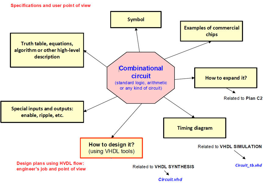
1.5. Design flow for inventing/creating/designing combinational circuits using VHDL
1.5.1. Specifications and theory, design concept map that connects with analysis ideas
1.5.1.1. Symbol or entity
1.5.1.2. Truth table
1.5.1.3. Example timing diagram
The main concepts related to our circuit consist of: symbol, truth table, timing diagram applying some values to prepare simulations, and theory, applications, context and examples commercial chips.
 |
Fig. 1. Symbol (entity) of a generalised combinational circuit. In CSD we propose up to fourteen architecture variations for inventing logic functions using VHDL or programming languages. |
1.5.2. CSD design plans or strategies to be used with VHDL or C language EDA tools
| Strategies for designing combinational circuits |
Plan A: structural, equation-based translation to VHDL in a single file (flat design)General ideas on designing combinational circuits using networks of logic gates covered in P1. 1) Canonical equations: sum of minterms. The truth table equation. 2) Canonical equations: product of maxterms. The truth table equation. 3) Minimised equations: SoP, the output from Minilog.exe. Used in sPLD-CPLD macrocells. 4) Minimised equations: PoS, Minilog.exe output results. 5) Modified equations to use only-NOR logic gates (universal gate). 6) Modified equations to use only-NAND logic gates (universal gate). 7) Mixing equations of any kind.
Plan B: behavioural, direct truth table/algorithm translation to VHDL in a single file (flat design)Covered from P2 where we start classifying standard logic circuits. 8) Translating the truth table directly to VHDL or to an algorithm represented by a flowchart.
Covered in P9 as an easy way to introduce microcontroller programming in C and basic I/O. 9) Translating the truth table directly to C language (or Python) as software to be executed in a microcontroller.
Plan C1: hierarchical structure of components (flat design, single-file)10) Not practical, and not used in CSD Chapter 1. Indeed, we use it only for describing FSM architecture in Chapter 2.
Plan C2: hierarchical structure of components, multiple-file designCovered in P3) where large and chained circuits are explained: 11) The method of decoders (MoD) 12) The method of multiplexers (MoM) 13) Circuit expansion. Most of circuits that deal with n-size vectors can be organised using identical chips or similar ones chained by means of a given pattern (i.e. carry in, carry out; enable in , enable out) using special inputs and outputs. For instance, we can invent an Enc_4_10 using Enc_2_4. Covered in L5.4 were memory components are introduced: 14) The method of ROM/RAM memory chips or lookup tables (FPGA - LUT)
|
1.5.2.1. VHDL plan A: structural/equations single-file strategies
1.5.2.1.1. Canonical equations: sum of minterms or product of maxterms.
Project tutorial #1: Two circuits from the Circuit_W truth table. |
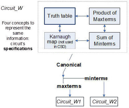 |
Fig. 2. Circuits W1 and W2 from the canonical equations of Circuit_W. |
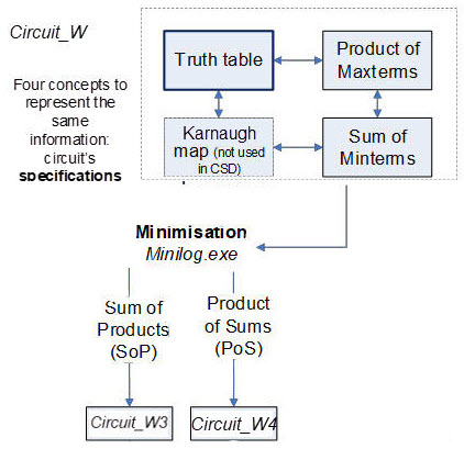
1.5.2.1.2. Minimised equations: SoP or PoS
- Espresso heuristic algorithm: Minilog.exe (we use Notepad++ as enriched text editor for writing text tables).
- Truth table translated to Minilog text input format (".tbl")
- Minilog minimisation results: SoP or PoS logic equations and equation converter
Project tutorial #2: Two circuits from the Circuit_W truth table. |
|
Fig. 3. Circuits W3 and W4, minimised equations from the Circuit_W truth table. |
Activity #1: Specifications: Invent the fourth version of Circuit_W from its truth table using minimised PoS (one of the possible circuits using structural plan A).
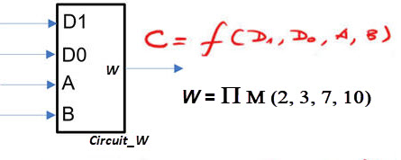 |
Fig. 1. Circuit_W symbol and truth table. |
Plan: Draw as a flowchart the procedure you will follow to obtain your solution.
Project location: C:\CSD\P1\Circuit_W\PoS\(files).
 |
Fig. 1. Simplified planning ideas to create Circuit_W from the minimised PoS. |
Development. Run Minilog and simplify using single output mode (SoM), equation output format, and choose PoS. Draw the logic circuit.
Test: Use Proteus or WolframAlpha (for instance, adapting a LAB1.1 tutorial) to check the truth table of this circuit or compare your results with your team mates.
Activity #2:
Specifications Design the SoP minimised circuit from the truth table deduced in this previous activity.
Some hints to start.
| Home Term 26/27-Q1 Contact Products Electronic devices and companies Software Books Magazines Instruments DEE Library EETAC DEEL |

|
|
| Web activa des de 09/2001, @ F. J. Robert, Web editat amb Microsoft Expression Web 4. El contingut és un complement als materials d'estudi del curs Circuits i Sistemes Digitals disponibles al campus digital Atenea. Llicència:Reconeixement 4.0 Internacional de Creative Commons |