|
|
Bachelor's Degree in Telecommunications Systems and in Network Engineering |
|
L3.3: Designing logic functions using plan C2: MoD, MoM [P3] Method of decoders (MoD) and method of multiplexers (MoM). |
[6 Oct] |
1.5.2.4. Plan C2: hierarchical design multiple-file (components and signals)
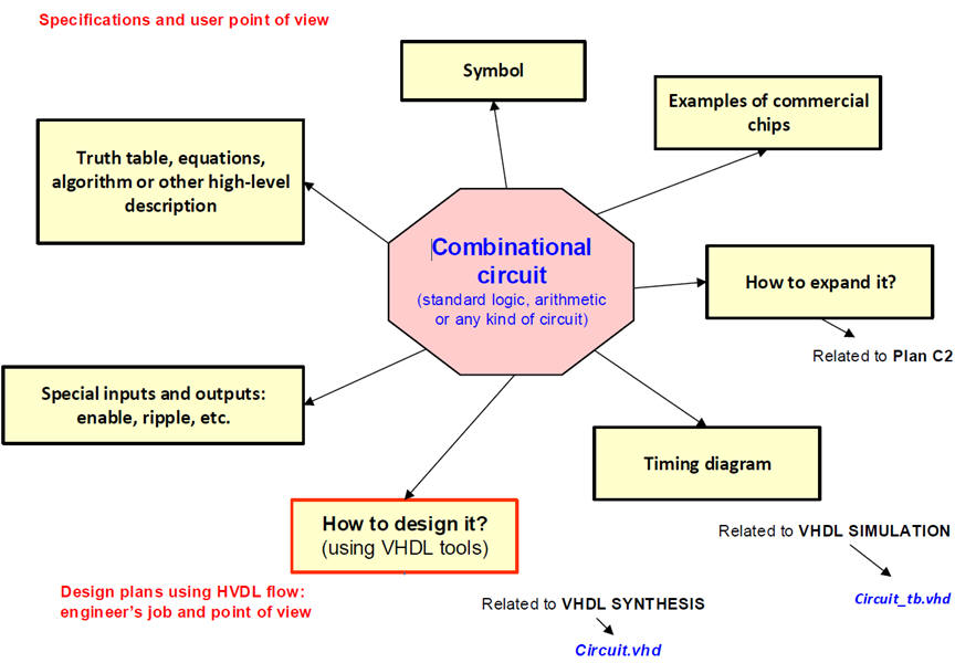
Since now we have studied several strategies to implement logic functions based on canonical equations (maxterms or minterms), minimised equations (SoP or PoS), only-NOR or only-NAND transformations, or even any combination of equations. All of them related to a given circuit structure or plan A. Other methods are related to plan B: capturing the truth table or interpreting it as a flowchart.
1.5.2.4.2. Method of decoders (MoD)
Now, we will implement logic circuits using hierarchical structures plan C2 based on decoder components. Decoders are standard logic components explained in L2.3 the properties of which makes simple the implementation of logic functions.
How does the method of decoders for implementing logic functions work?
Example design: Circuit_C using MoD.
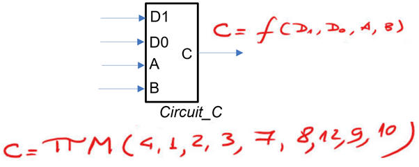 |
Fig. 1. Circuit_C symbol and truth table. |
Hierarchical structure Circuit_C:
 |
|
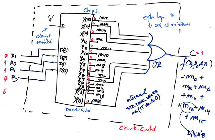
Fig. 2. Circuit_C hierarchical structure using a decoder component. |
Example design: Circuit_K using the MoD.
Example design: 1-bit full adder (Adder_1bit) using MoD.
1.5.2.4.3. Method of multiplexers (MoM)
Multiplexers are standard logic components explained in L2.1. How does the method of multiplexers for implementing logic functions work?
A) Draw the symbol and expand the truth table to show all combinations
B) Section the truth table accordingly to the number of MUX channels
C) Connect the selection inputs to circuit inputs assigning inputs from from left to right.
D) Solve the remaining combinational logic that has to be attached to each channel
Example design: Comb_circuit using MoM and MUX_8, MUX_4 and MUX_2.
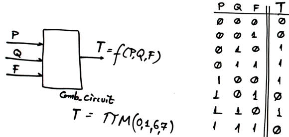 |
Fig. 3. Comb_circuit symbol and truth table. |
Fig. 4 shows the solution when designing the Comb_circuit uisng the MoM and a MUX_8.
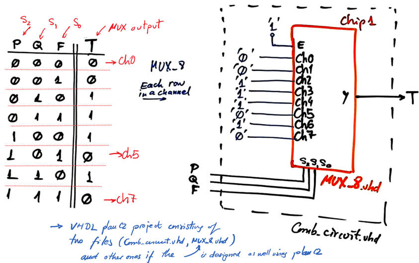 |
| Fig. 4. Comb_circuit using MoM and a MUX_8. |
Fig. 5 shows the solution when designing Comb_circuit using MoM and a MUX_4.
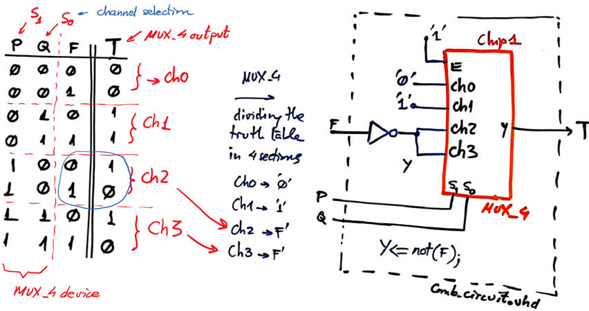 |
Fig. 5. Comb_circuit using MoM and a MUX_4. |
Fig. 6 shows the solution when designing Comb_circuit using MoM and a MUX_2.
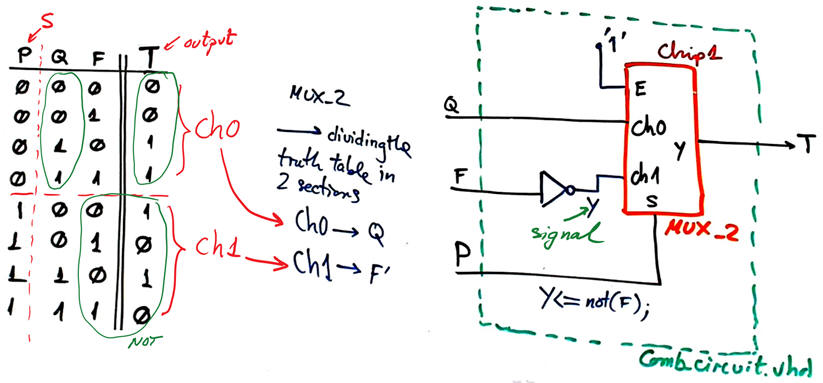 |
Fig. 6. Comb_circuit using MoM and a MUX_2. |
A good idea now is to translate to VHDL the schematics in Fig. 4 "Comb_circuit.vhd", Fig. 5 "Comb_circuit.vhd" and Fig. 6 "Comb_circuit.vhd", and run synthesis and simulation "Comb_circuit_tb.vhd" to check whether the circuits generates the truth table in Fig. 3. As usual, place each project in a different folder:
- C:\CSD\P3\Comb_circuit_MoM_MUX_8\(files)
- C:\CSD\P3\Comb_circuit_MoM_MUX_4\(files)
- C:\CSD\P3\Comb_circuit_MoM_MUX_2\(files)
Example design: 3-bit even parity generator using MoM and a MUX_2.
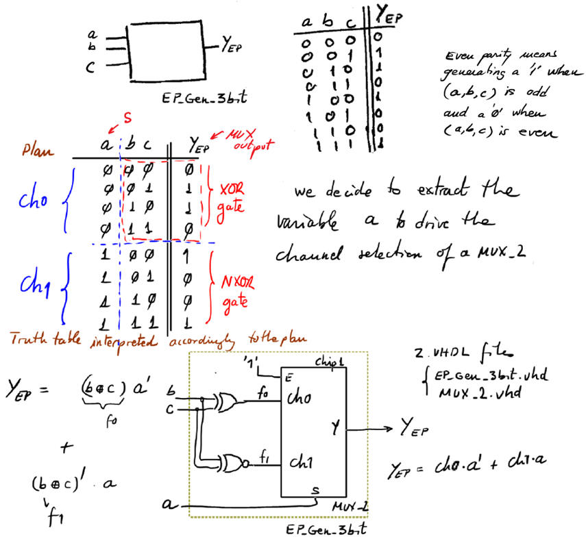 |
Fig. 1. Discussion on how to implement the 3-bit even parity generator using MoM and a MUX_4. |
Example design: Circuit_C using MoM and a MUX_4.
|
|
Fig. 1. Circuit_C symbol and truth table. |
A solution using MoM and MUX_4 is represented in Fig. 2.
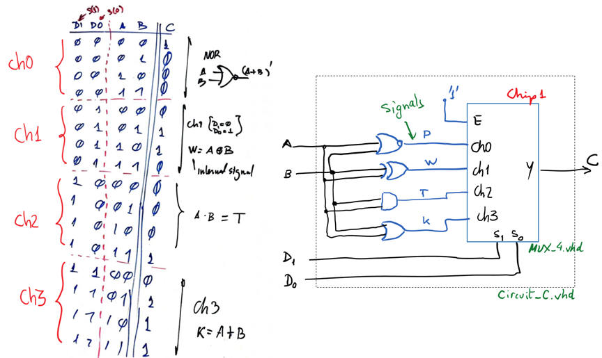 |
Fig. 2. Proposed solution for Circuit_C |
Example design:
- Comp_1bit using MoM and MUX_2 (GT), MUX_4 (EQ) and MUX_8 (LT)
Example design:
- 1bit_adder based on the MoM using MUX_2 for So and MUX_4 for Co. Lab3.
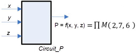
Activity #1: Design the Circuit_P using plan C2 and the MoD. Generate the decoder component expanding smaller blocks of the same kind. How many VHDL files are required to implement this circuit?
Remember that a project as a class activity requires this initial paper work:
(1) Specs & theory (our map of concepts)
(2) Planning. How we solve design projects using VHDL tools? Which design strategy to translate into VHDL files? a) sketch (enough for exams and peer discussion) and b) totally annotated schematic required to start development
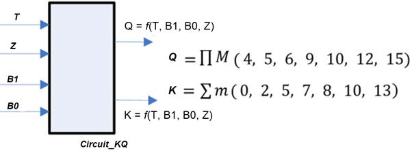
Activity #2: Design the Circuit_KQ using plan C2 and these two alternative hierarchical architectures:
- MoD
- MoM and a MUX_4 for Q and a MUX_2 for K.
Remember that a project as a class activity requires this initial paper work:
(1) Specs & theory (our map of concepts)
(2) Planning. How we solve design projects using VHDL tools? Which design strategy to translate into VHDL files? a) sketch (enough for exams and peer discussion) and b) totally annotated schematic required to start development
Activity #3: Design the Sub_1bit proposed in D1.13 using plan C2 and one of these two alternative hierarchical architectures:
-
MoD. Continue the exercise designing the component using plan C2 and chip expansion techniques: Dec_3_8 using Dec_1_2
-
MoM and a MUX_4 for do. MoM and a MUX_2 for bo.
Remember that a project as a class activity requires this initial paper work:
(1) Specs & theory (our map of concepts)
(2) Planning. How we solve design projects using VHDL tools? Which design strategy to translate into VHDL files? a) sketch (enough for exams and peer discussion) and b) totally annotated schematic required to start development
| Home Term 26/27-Q1 Contact Products Electronic devices and companies Software Books Magazines Instruments DEE Library EETAC DEEL |

|
|
| Web activa des de 09/2001, @ F. J. Robert, Web editat amb Microsoft Expression Web 4. El contingut és un complement als materials d'estudi del curs Circuits i Sistemes Digitals disponibles al campus digital Atenea. Llicència:Reconeixement 4.0 Internacional de Creative Commons |