|
|
Bachelor's Degree in Telecommunications Systems and in Network Engineering |
|
|
| |||
|
|
P_Ch2 Questions and answers |
|
|
| |||
Consider the discussions in this page as an addendum to your PLA assignments. This edited Q&A comes from meet sessions, emails, phone calls, and class and office time with many students. Thus they have significant value and will help you to save study time. You may imagine a class-group working cooperatively in a weekly basis with the objective of solving our projects as better and faster as we can.
-
PLA6_7 Implementing FSM, counters, registers, datapath, dedicated processors
Question: I can't find where the Johnson counter and the Gray code are.
Answer: Well, all these binary codes: radix-2, Gray, one-hot, Johnson, etc., are standard binary codes used in many applications. Google these names and you will find pages with information.
Question: I don't know how to do the CLK process. I deduce that the counter Johnson putting four T_FF in series, since it is what I have found on the internet as you can see in this image. I also have the doubt of whether the program in VHDL have to do it with chips D_FF or T_FF.
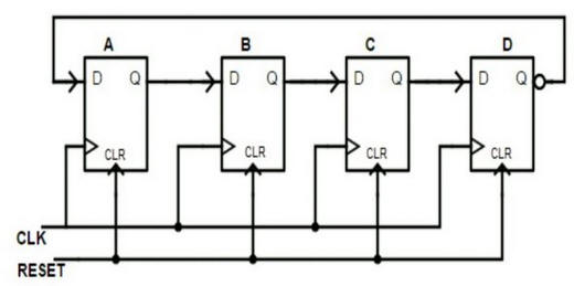
Answer: If you have to design a Johnson counter using our FSM approach, you may use internet for finding simply what is the Johnson code and so determine what outputs are generated at each state. In this way you will fully comprehend the specifications of the application that you are designing. Inventing circuits in CSD is 1-2-3-4-5 as usual, and in this case, applying our FSM method from a) to n). And all of this, as you can guess, only after having completed LAB6 reference tutorials and studied P6 highlighted project, because PLA6 is simply a systematic repetition and adaptation.
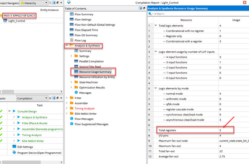
Question: Where to find the information on the number of D_FF used in the design if the target chip is MAX II?
Answer: You can find it in a summary file generated by the analysis and synthesis process:
Question: I have a question about Timing Analyzer. I did all of the simulations and I am not sure if my results are correct because the report datasheet is not similar to the one we did in previous projects. Is it because I made a mistake or is it correct?
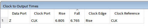
Answer: Yes here in Chapter 2 we are not that much interested in propagation delays of gates tP from any input to any output as we were in Chapter 1, but now our interest relies on "how long does it take to change outputs synchronously with CLK rising edges".
It seems ok, what I do is simply swap the columns in the spreadsheet: from CLK port to output data port because the meaning is clearer. It says that tCO = 6.8 ns, meaning that you can speed up your system CLK up to a maximum frequency of 147 MHz and the digital system is still working correctly.
Question: Our assignment is to built the roulette using shift registers, I want to understand more how to implement this kind of circuit because reading the indications are not clear.
Answer: The more time you spend on specifications the better. Study what is a shift register, for instance from this tutorial Shift_reg_4bit. Imagine the circuit from this perspective at the specifications level. Here, in your application, one key idea is how to expand it, the same approach that we used for Counter_mod16 and building larger counters. Study and find information on roulettes, the simplest ones, what kind of buttons and outputs they have, how they work.
You can use this shift register to invent using plan C2 a larger one (chip chaining or chip expansion). And then, I guess that the idea of a roulette is loading in parallel a single '1', and rotate it at high speed, for example meanwhile the player is pressing the button "play". Probably, when releasing the button, the '1' will be saved in anyone of the numbers. Or something like this to start. This project can be used as an starting point for discussing the generation of random numbers using digital circuits or computers.
Question: Discussing about the clock generator in the Counter_BCD_mod24, where do you want us to put it in the report and what do you want us to show about it?
Answer: You may think about a Counter_BCD_mod24_top that includes other components like CLK_Generator and (optionally) Hex_7seg_decoder if you like to present results in 7-segment displays. Something like this. As you see in P8 Timer highlighted project, CLK_Generator is designed internally as a component in an annex.
Question: I would want to ask about the Data_Reg_20bit, do we have to use the PlanY or PlanC2 using components such Counter_mod16?
Answer: If you have to invent large counters or large data or shift registers, it is better to use basic components like Counter_mod16 or Data_reg_4bit or Shift_reg_4bit, already solved in Digsys P7, and learn how to chain or expand them to design larger modules of the same kind, this is studying for exams at the same time that solving PLA7. But it it up to you, you can choose.
Question: I'm wondering if it is correct to use a Counter_mod16 and truncate it to 9? I mean, doing this: Digit tens: 0,0,0...,0,0, 1,1,1,1,...1,1,1,..., 5,5,5,...,5,5,5,0,0... Digit units: 0,1,2...,8,9, 0,1,2,3...,7,8,9,..., 0,1,2...7,8,9,0,1... So that when the digit arrives to 59 changes to 00.
Answer: Which PLA7 circuit was assigned to your group? Read and study in detail diagrams and ideas solved in class and available in digsys lessons and tutorial examples, because many times we have already discussed these ideas and probably you have class notes. If your question is on counter chaining and truncation, it was at lecture L7.3 where we studied in detail these concepts, and for instance P7 highlighted project shows you many details, pictures and diagrams. Probably your PLA7 is a simple repetition and adaptation on what is covered in class; this is why attending classes is such crucial in CSD.
Question: Regarding the video we are facing a slight problem with the duration, as it is a quite long project. We try to explain our design in the blackboard, the transition to VHDL code, Quartus synthesis, functional and gate-level simulation, etc.; the video gets a little bit longer. Is it okay if we exceed the time limit of 10 min?
Answer: This is a very good question, thank you. Well, this is the point. There is no need to explain everything. Oral presentations aim to be succinct and brief, focused on main points and ideas. Doctoral thesis may be abstracted in 10 min. if required. Presentations of scientific papers in most conferences are not much longer. Technical reports, on the other hand, may be as long and detailed as necessary (so that other engineers can repeat and validate or refute the experiments). The question is: how to explain my complex design work in 7 min to a technical audience? (7 minutes is ok because you are only two members)
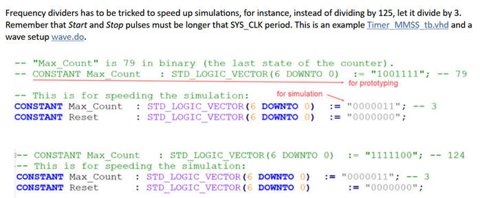
Question: How to speed up the simulations when including a CLK_Generator?. If the OSC_CLK_in = 50 MHz, every real-time second will require simulating 50 millions of CLK pulses. And this is going to slow simulations too much.
Answer: A good idea is to trick the frequency divider. If we want to generate CLK_200Hz_SQ, the required frequency divider chip is Freq_div_125000. The required Max_Count is 124999 = "11110100001000111" (17-bit vector). While simulating you can replace it by a simple division by 10 but keeping the same number of D_FF. Max_Count = 10 = "00000000000001010". In this way, the frequency divider will run much faster. The testing section of the P8 highlighted project shows this application.
Question: How to write PLA7 report?
Answer: The best way to report or present projects is thinking in what your audience will comprehend after reading or listening to you. In this course it is easy: one full project at a time (related to its state diagram).
And the advantage of designing using steps is this: they are different, separated, independent projects for building commercial products. For a given specifications, design step #2 or design step #3 projects will have more features / buttons / controls / outputs than the first project in design step #1, but this is the idea: the design approach used by commercial companies for conceiving, creating, manufacturing and selling new electronic appliances such mobile phones or TV sets every year.
We will plan projects using design steps and phases all the time. Steps will be for minor changes, small modifications; phases for new components or architectures, large improvements or enhancements.
| Home Term 26/27-Q1 Contact Products Electronic devices and companies Software Books Magazines Instruments DEE Library EETAC DEEL |

|
|
| Web activa des de 09/2001, @ F. J. Robert, Web editat amb Microsoft Expression Web 4. El contingut és un complement als materials d'estudi del curs Circuits i Sistemes Digitals disponibles al campus digital Atenea. Llicència:Reconeixement 4.0 Internacional de Creative Commons |