|
|
Bachelor's Degree in Telecommunications Systems and in Network Engineering |
|
Lecture 3 |
L5.3: Flip-flop specifications and applications [P5] - D-type, JK, and T flip-flops |
[3 Nov] |
2.3.6.2. Data flip-flop (D_FF)
2.3.6.2.1. Function table, state diagram, timing diagram
This is the full tutorial on designing our D_FF as another example of application of the FSM architecture, even if it is a simple two-state machine. In the development section of the tutorial you will find the VHDL files that translate the behaviour of this component.
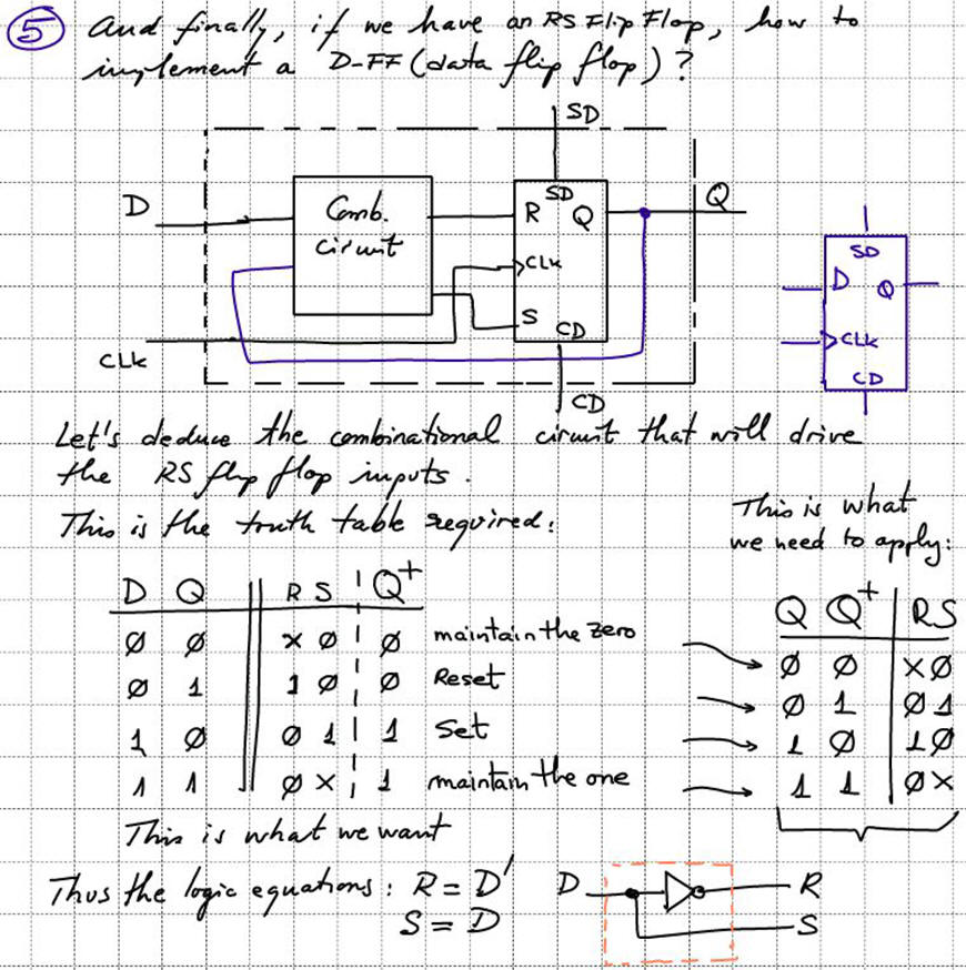
2.3.6.2.2. Deducing D_FF from RS_FF
As an alternative, we can add a bit of theory using plan C2 to imagine D_FF from the previous RS_FF.
2.3.6.2.3. Commercial chip
A standard commercial D_FF is the 74HCT273. or the 74LS74.
2.3.6.3. JK flip-flop (JK_FF)
2.3.6.3.1. Function table, state diagram, timing diagram
This is the full tutorial on designing our JK_FF as another example of applying the FSM architecture, even if it is a simple two-state machine. In the development section of the tutorial you will find the VHDL files that translate the behaviour of this component.
2.3.6.3.2. Commercial chip
Classic chips of this kind are HEF4027B and 74HCT73.
2.3.6.4. Toggle flip-flop (T_FF)
2.3.6.4.1. Function table, state diagram, timing diagram
This is the full tutorial on designing our T_FF as another example of applying the FSM architecture, even if it is a simple two-state machine. In the development section of the tutorial you will find the VHDL files that translate the behaviour of this component.
2.3.6.4.2. Frequency divider by two
This is a simple and typical application of the T_FF, imagining it as a CLK's frequency divider by 2. We will take advantage of this circuit when inventing CLK generator circuits in P8 for squaring pulsed signals.
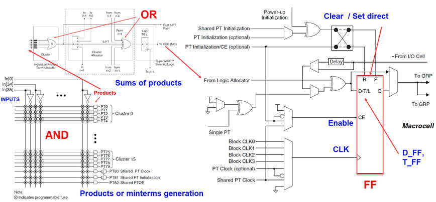
2.3.6.5. Use of flip-flop in (PLD) and FPGA.
Each logic elements/block/cell has two main components: (1) configurable combinational circuit and (2) flip-flop.
Programmable logic devices (PLD) implements logic functions using SoP or sums of minterms. Additionally each cell contain a flip-flop. For instance, the Lattice Semiconductor CPLD ispMACH4128V contains 128 logic blocks and macrocells. Each macrocell includes a configurable register D_FF along with some logic for CD, SD, CLK and enable.
2.3.7. Timing parameters: Time clock to output (tCO). Set-up time (tSU), hold time (tH). Maximum CLK frequency (fCLK_max).
The schematic used in this explanation uses a D_FF, but all the concepts are generalised for all flip-flop. As we have discussed, the basic idea behind the flip-flop function table is that the next output value (Q+) after the CLK's rising edge depends on the sampled values of their input control signals.
Therefore, the input data D must be steady at least tSU ns before the CLK event. And in the same way, D must be kept steady at least a minimum tH time. Consequently, the minimum duration of a signal D to be correctly acquired must be larger than (tSU + tH). Chip technology and logic families characteristics will determine the time resolution of a given digital application.
Observing the waveforms, we can also infer that the maximum CLK frequency never must be higher that the limit imposed by the technology. TCLK_min > tCO, or fCLK_max < 1/tCO
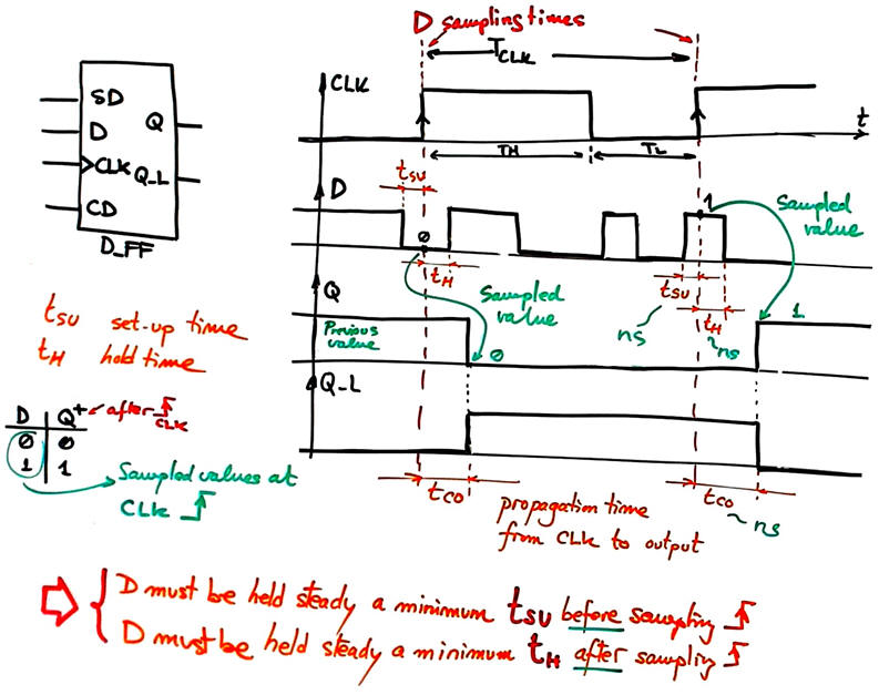
Considering a typical chip 74HCT74 characteristics tSU = 5 ns, tH = 3 ns, fCLK_max = 1/18 ns = 55 MHz. A signal D pulse shorter than 8 ns cannot be detected by this logic family. However, practically, it is the TCLK_min that fixes time resolution: signal pulses shorter than 20 ns will not be sampled or captured correctly; they will be considered like noise or glitches, as we have represented in many timing diagrams.
A reference for these timing parameters (ref.).
2.3.8. Analysis of asynchronous and synchronous circuits based on flip-flops and logic
NOTE. Analysis of circuits with memory cells and gates (such the one presented in P5 is covered in several tutorial projects, where we propose three analysis methods:
2.3.8.1. Method I: Handwritten pen-and-paper analysis and discussion.
2.3.8.2. Method 2 Proteus simulation
2.3.8.3. Method 3 VHDL synthesis and simulation.
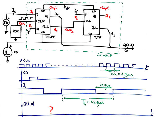
Thus, let us repeat and apply again the same three P1 analysis methods. This below is another example circuit:

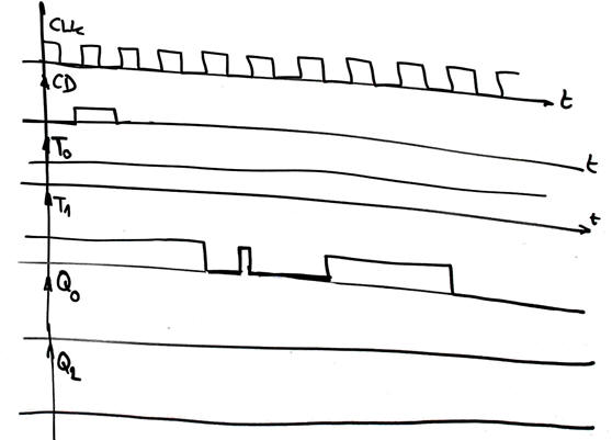
Specifications: Find the timing diagram and infer which binary codes are available at output W(2..0). Imagine that J is a 70% duty cycle waveform of 230 Hz, and fCLK = 2.5 kHz.
Planning: You can use the three analysis methods and compare results.
You can organise several steps:
Step #1: Only the first JK_FF Chip0
Step #2: Only Chip0 and Chip1
Step #3: The complete circuit
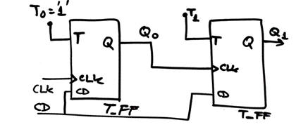
Activity #1: Deduce the output Q(1..0) of the Circuit_P below using method I and (method II or method III) so that you are able to check your results. J1 and CD are external waveforms from signal generators that are not synchronised to the CLK.
Plan several steps to make the project easier and valid for working in group. Example of checklist to prepare and self correct your materials.
The basic idea to organise this activity is to prepare good material to be able to solve more complex projects.
Step #1. Analyse using the the three methods proposed a circuit with a single flip-flip and also gates if liked. So that the many new concepts and devices are understood: CLK signal, period and frequency, rising and falling edges; CD clear direct initialization pulse, why it is required and how it is used, which circuit can generate it; what signals have priority, which signals are asynchronous; which are the control signals for each FF, what is the meaning of the future state, when does it happens, what is the meaning of memorising a bit value; what happens when the control signals are switching just on CLK's the rising edge; which components and integrated circuit can I simulate Proteus: where are the VHDL models for solving the circuit using method III, which is the schematic of the testbench fixture, etc.
Step #2. It may be to analyse a circuit with two CLK's: when each FF will update its state;
Step #3. It may be to repeat and try to apply all you knowledge to the circuit in the figure.
Activity #2: Deduce the outputs of the circuit below:
| Home Term 26/27-Q1 Contact Products Electronic devices and companies Software Books Magazines Instruments DEE Library EETAC DEEL |

|
|
| Web activa des de 09/2001, @ F. J. Robert, Web editat amb Microsoft Expression Web 4. El contingut és un complement als materials d'estudi del curs Circuits i Sistemes Digitals disponibles al campus digital Atenea. Llicència:Reconeixement 4.0 Internacional de Creative Commons |