|
|
Bachelor's Degree in Telecommunications Systems and in Network Engineering |
|
PLA2_3: Designing arithmetic and logic circuits |
Specifications
Prerequisite training: Study in detail and execute in your computer these tutorials P1 design, P2, P3, Lab 2, Lab 3 before attempting this PLA.
Design three projects, each one based on a different architecture: plan A: structural, equations; plan B: behavioural, high-level; plan C2: structural hierarchical.
| NOTE: We use your discussion and feedback to clarify and better organise project specifications editing immediately these pages, thus you may expect changes on the assignment pages for the good. Notify us whatever detail that is not clear enough. This is a way to put into practice and reinforce teamwork and cooperation between all the company engineers. |
| Example of group assignments and options | |||||
| Project numbers | Circuit entities | Plan | FPGA target chip | Operands for timing diagrams and test benches | |
| Group 1 | D1.7 | Bar_28LED |
Top entity Plan C2 Bar_28_LED_dec Plan A (PoS) Bar_28_LED_dec Plan B |
MAX10 | |
| Group 2 | D1.6 | Tank_20level_meter | Top entity Plan C2 Tank_10level_meter Plan A (PoS) Tank_10level_meter Plan B |
MAX II | |
| Group 3 | D1.5 | 32-key gamer keypad Enc_32_5 |
Top entity Plan C2 option #1 using Enc_8_3 Enc_8_3 Plan A (PoS) Enc_16_4 Plan B |
Cyclone IV | |
| Group 4 | D1.7 | Bar_28LED |
Top entity Plan C2 Bar_28_LED_dec Plan A (SoP) Bar_28_LED_dec Plan B |
MAX10 | |
| Group 5 | D1.6 | Tank_20level_meter | Top entity Plan C2 Tank_10level_meter Plan A (SoP) Tank_10level_meter Plan B |
MAX II | |
| Group 6 | D1.5 | 32-key gamer keypad Enc_32_5 |
Top entity Plan C2 option #2 using Enc_16_4 Enc_8_3 Plan A (SoP) Enc_16_4 Plan B |
Cyclone IV | |
| Group 7 | D1.7 | Bar_28LED |
Top entity Plan C2 Bar_28_LED_dec Plan A (PoS) Bar_28_LED_dec Plan B |
MAXII | |
| Group 8 | D1.6 | Tank_20level_meter | Top entity Plan C2 Tank_10level_meter Plan A (PoS) Tank_10level_meter Plan B |
Cyclone IV | |
| Group 9 | D1.5 | 32-key gamer keypad Enc_32_5 |
Top entity Plan C2 option #1 using Enc_8_3 Enc_8_3 Plan A (PoS) Enc_16_4 Plan B |
MAX10 | |
Follow this rubric for writing reports. This group submission at Atenea includes the report in a PDF file, the zipped project, a 10 min. max video presentation and also your self-assessment.
| NOTE: This project will be continued in PLA4 adding time measurements for real technology. And you will have the opportunity to complete the top entity if something is not yet fully operational. |
How to organise and handwrite the plan C2 project:
1. Specifications and theory
-
Original handwritten materials on symbol, truth table, timing diagram and other explanations on data types and operations to be performed.
-
Explain the meaning and the function of each input and output and the data range.
-
Include examples on how the circuit operates, use the corresponding radix for easy interpretation of the operands and results.
NOTE: You better add theory, class-notes or other learning materials in section 1 on specifications in one of your projects. Explain, discuss and try to locate in CSD lessons or laboratory tutorials the concepts and tools used in these PLA plans and developments, so that you are sure that these materials will help you to study and solve similar problems for Exam 1. |
2. Planning
| NOTE: One project at a time, starting from the simplest. Solving the next project after having corrected errors from the previous one. Do not worry much if you cannot complete the full PLA2_3 or by the due date it still does not work satisfactory. This PLA2_3 will be continued in PLA4, where you will be able to include corrections or improvements after our feedback. |
-
Original handwritten sketches, explanations and VHDL-ready schematics on how your plan C2 circuit is conceived, the proposed hierarchy of components, signals, number of VHDL files, project folders and names, etc.
-
On cooperative work:
NOTE: This is cooperative group work. You must explain in the planning section of your report and video, who is in charge of each section, who is leading the tasks, who is developing the components or sections, who is measuring or testing, etc. It is fundamental in order to obtain good assessments that you explain very well which is the contribution to the final project of each one of the group members. |
-
Explain how your large hierarchical top entity project is divided in interconnected components (to be designed separately in annexes if they cannot be found in products).
-
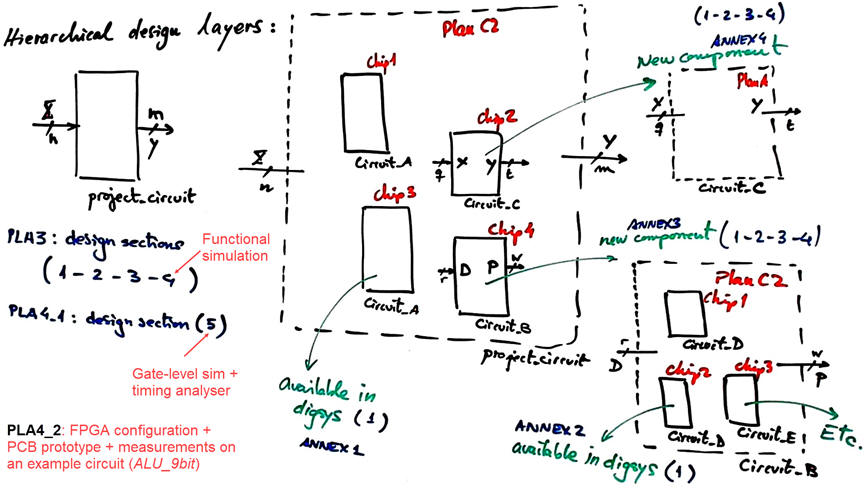
Explain which component (project) you will solve (1-2-3-4) firstly to get some practice with the tools and the plan C2 before designing other components or assembling the top entity. This slide may give you an idea:
3. Development
-
Top project development in Quartus Prime for a target FPGA chip.
-
Printings and handwritten discussions of RTL and technology schematics.
-
How many FPGA resources (logic cells, logic elements, etc.) are used?
4.Test and verification
-
Testbench fixture schematic.
-
Proposed stimulus testbench process.
-
Printings and handwritten discussions on results.
-
Add your conclusions on the project and on what has been learned. Remember that your self-assessment is expected to be submitted as well at the Atenea platform.
5. Annexes
-
If you invent a new component that is not available in products, the best way to report it is as an annex organised as a complete project 1-2-3-4.
-
If you use VHDL files from a component already available in products, you simply need to describe its symbol and truth table in a single sheet(specifications), as a way for you to keep studying for exams.
Notes on video presentations: 10 min. max., 3 - 4 min. each participant.
The idea of the video presentation is different from the written report and has its own particular objective: develop your oral communications skills in our engineering context in a way a large audience can grasp the main details of your project. Put in motion your communication skills that you will continue to practise and improve through PLA6_7 and PLA10_11. We will focus assessment in how you are organising the presentation, how confident you are in front of the camera, time sharing among students, support materials and audio and video quality. This is an example of final PLA11 presentation. A good idea is to submit a meet recording or equivalent.
| ===> Do not browse your report pages when presenting, prepare some slides instead. |
| Home Term 26/27-Q1 Contact Products Electronic devices and companies Software Books Magazines Instruments DEE Library EETAC DEEL |

|
|
| Web activa des de 09/2001, @ F. J. Robert, Web editat amb Microsoft Expression Web 4. El contingut és un complement als materials d'estudi del curs Circuits i Sistemes Digitals disponibles al campus digital Atenea. Llicència:Reconeixement 4.0 Internacional de Creative Commons |