|
|
Bachelor's Degree in Telecommunications Systems and in Network Engineering |
|
L5.2: RS flip-flops [P5] On the internal architecture of an RS flip-flop, CLK and clear direct (CD) concepts |
[3 Nov] |
2.3. Flip-flop. Synchronous 1-bit memory cell
Flip-flops are basic building blocks for digital systems. They are documented everywhere.
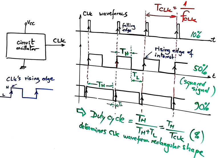
2.3.1. The concept of CLK signal. Synchronicity
In a digital system, outputs (Y) and internal states (S) update to the future value only on the CLK's rising edge transition, this is the idea of synchronicity or synchronous digital system.
Digital CLK oscillators generates rectangular signals for running digital systems. One rising edge per period.
2.3.2. CLK distribution.
2.3.3. CLK circuits
2.3.2.1. RC circuit
2.3.2.2. Integrated circuit 555 oscillator
2.3.2.3. Quartz crystal oscillator
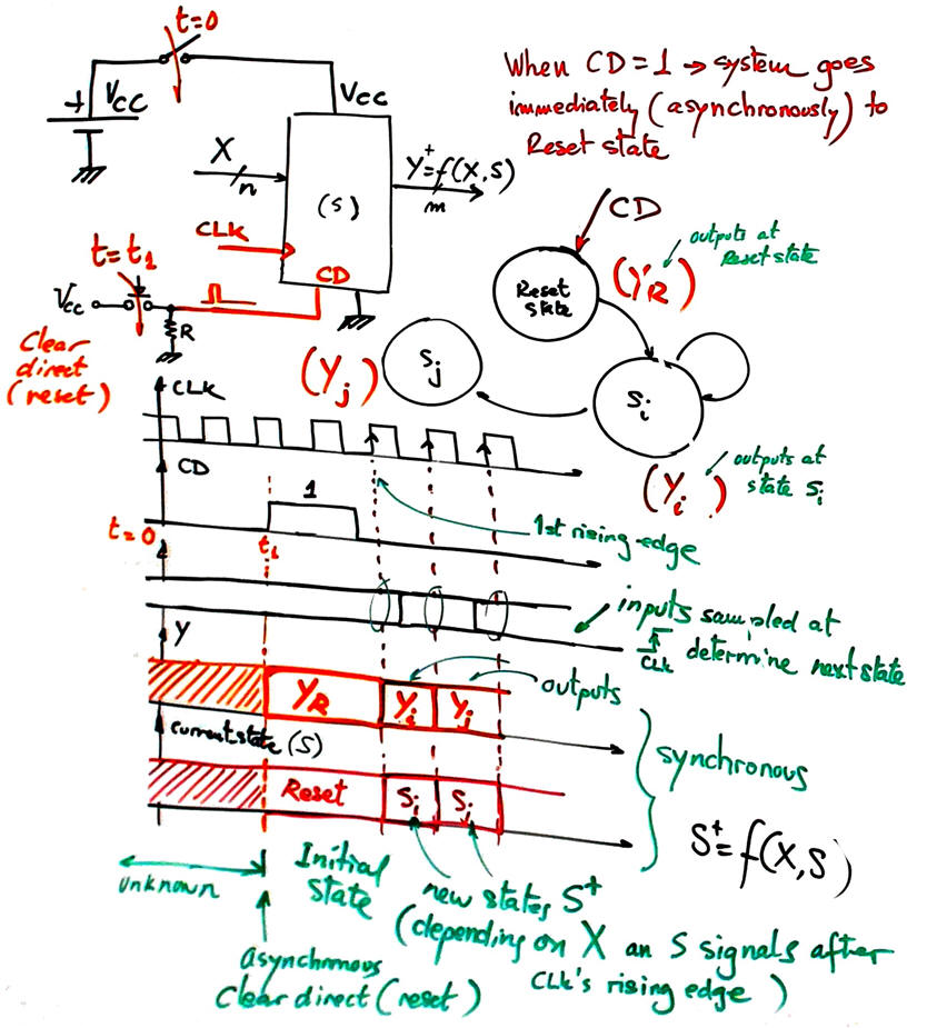
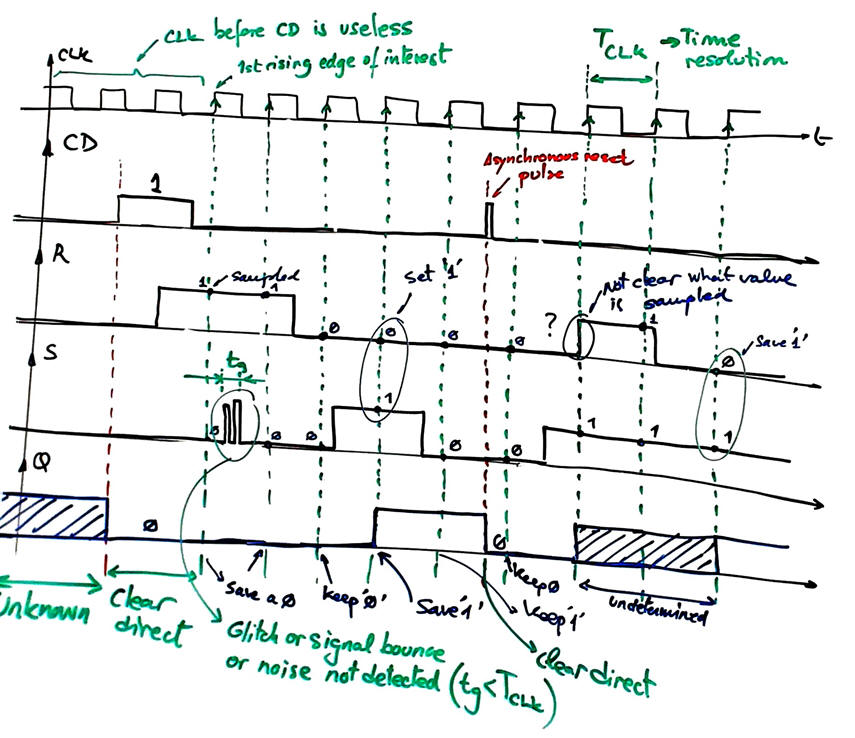
2.3.4. The concept of clear direct (CD), asynchronous reset or master reset.
In a digital system time starts when turning ON the power supply at t = 0. System internal state (S) and outputs (Y) remains undetermined, unknown or unpredictable until a reset or clear direct (CD) button is clicked at t = t1. While CD is set high, the systems remains at its initial state. Once CD is low the system starts updating outputs (Y) and internal states (S) after each CLK's rising edge.
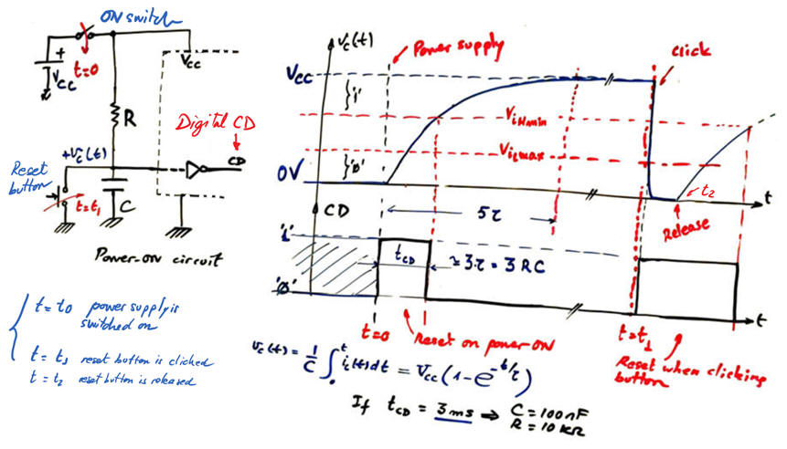
2.3.5. Automating system initialisation: power-ON reset.
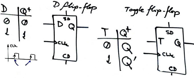
2.3.6. Standard flip-flops
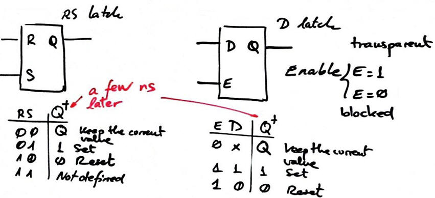
In previous lesson we studied asynchronous latches RS_latch and D_Latch
Now we can present common types of synchronous flip-flops, 1-bit memory cells: RS_FF, D_FF, JF_FF and T_FF .
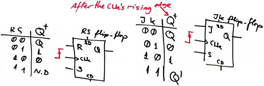
2.3.6.1. RS flip-flop (RS_FF)
2.3.6.1.1. Function table, state diagram, timing diagram
Run in Proteus the RS_FF.pdsprj example to grasp differences with respect a latch. What is the meaning of sampling input values?
2.3.6.1.2. Deducing RS_FF from RS_latch, CLK's rising-edge detector
Proposing an RS_FF circuit from plan A: how to deduce an RS_FF from an RS_latch?
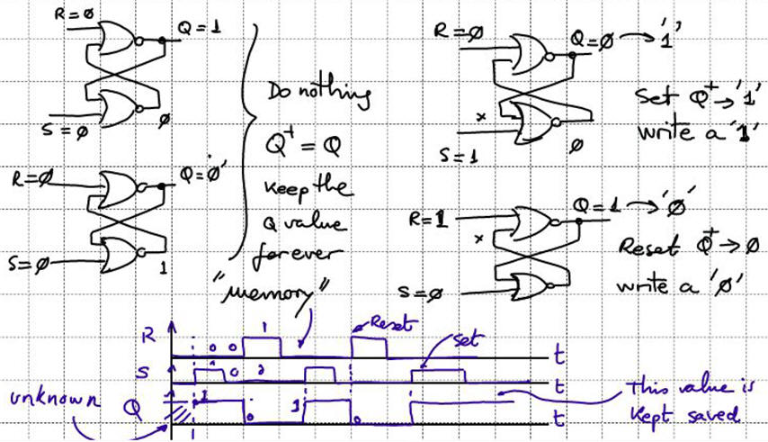
1. RS_latch operation
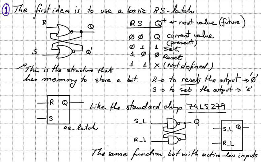
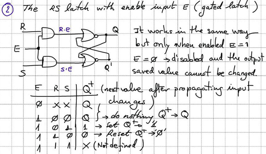
2. From RS_Latch to gated RS_Latch
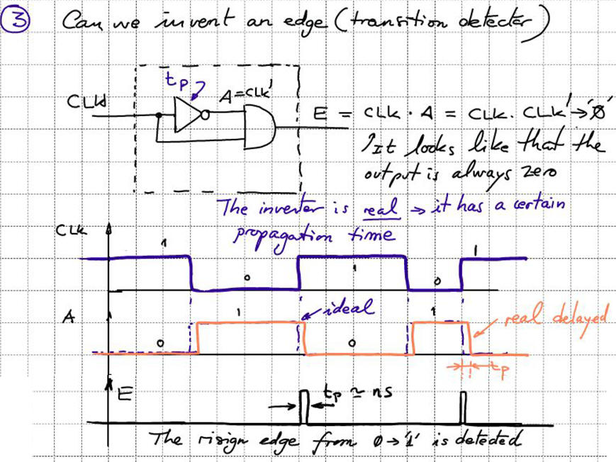
3. Edge detector circuit to convert CLK input into enable signal input
4. From gated RS latch to RS_FF
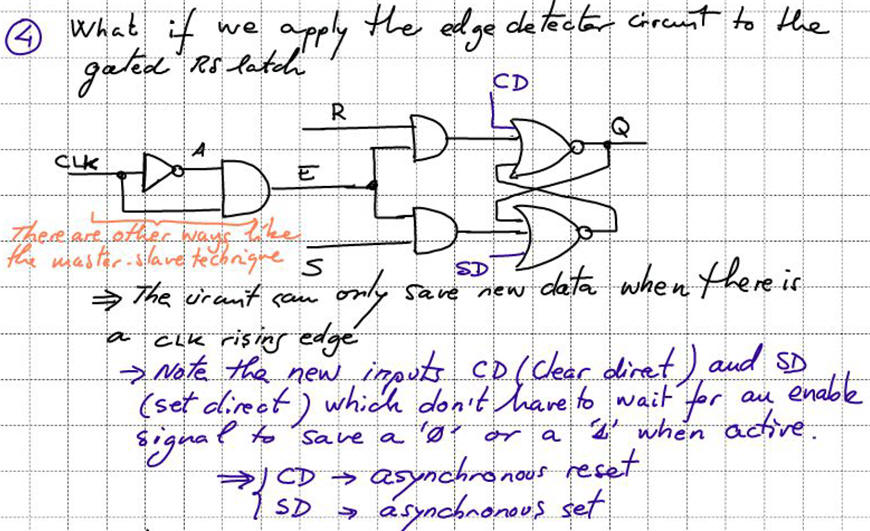
This an idea on how a CLK rising edge can trigger the sampling of inputs. Other circuits are proposed in literature, for instance master-slave configuration.
Fortunately, we well describe such components using a much simple, easier and repetitive behavioural approach, leaving to EDA tools the synthesis of such memory cells in FPGA fabrics.
2.3.6.1.3. Commercial chip
A classic chip is HEF4027B.
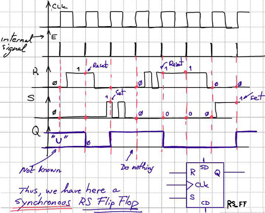
Activity #1: A RS_FF is driven by the following waveforms. Deduce and explain the output signal.
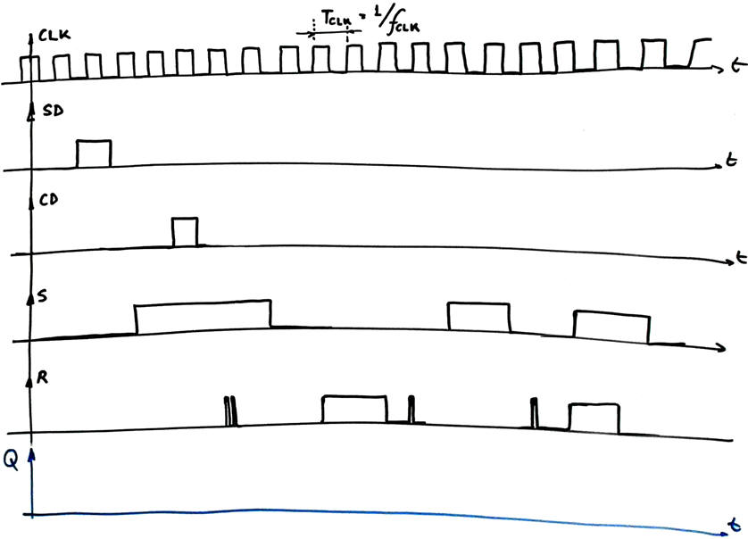
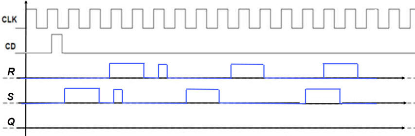
Activity #2: Analyse the following RS_FF applying its function table.
| Home Term 26/27-Q1 Contact Products Electronic devices and companies Software Books Magazines Instruments DEE Library EETAC DEEL |

|
|
| Web activa des de 09/2001, @ F. J. Robert, Web editat amb Microsoft Expression Web 4. El contingut és un complement als materials d'estudi del curs Circuits i Sistemes Digitals disponibles al campus digital Atenea. Llicència:Reconeixement 4.0 Internacional de Creative Commons |