|
|
Bachelor's Degree in Telecommunications Systems and in Network Engineering |
|
Lecture 2 |
L7.2: Registers [P7] Standard sequential blocks: Synchronous data and shift registers (Plan Y and plan C2) |
[13 Nov] |
2.7.5. n-bit data register: for example Data reg_4bit
2.7.5.1. Symbol, function table, parallel load, timing diagram, state diagram, commercial chips
This is the key component for saving data.
2.7.5.2. Plan Y
2.7.5.3. Plan C2 using components (Counter_mod16 or Data_reg_4bit)
As an alternative, figure out how to plan a Data_reg_16bit using plan C2 and Data_reg_4bit components
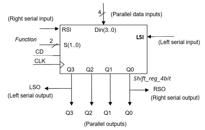
2.7.6. n-bit shift register: for example Shift reg_4bit
2.7.6.1. Symbol, function table, parallel load, timing diagram, state diagram, commercial chips
2.7.6.2. Plan Y
Type 74LS94, where the parallel input - parallel output mode of operation is identical to the data register.
2.7.6.3. Plan C2 using components Shift_reg_4bit
Figure out how to plan a Shift_reg_32bit using plan C2 and Shift_reg_4bit components
2.7.7. Barrel p_shift register n-bit. For example Barrel_3_shift_reg_21
2.7.7.1. Symbol, function table, parallel load, timing diagram
2.7.7.2. Plan Y
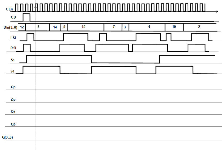
Activity #1: Draw an example timing diagram for the Shift reg_4bit. For instance, use these stimulus pdf to drive the circuit.
1. Specifications: Symbol, function table, example of timing diagram, example commercial chip, etc.
2. Planning the internal design of the component as a FSM using our recipe. Sections, c, d, e, f, g. Organising the internal architecture using plan B in a single plan C1 VHDL file allow us to easily expand this component to any size n. Read and study how it is done in the tutorial Shift reg_4bit.
Optional as class activity (only if you have study time available to spare on it). Synthesise and test the circuit completing the procedure sections from h to n. NOTE that you can not develop VHDL files unless all the diagrams and tables from sections c, d, e, f, g are completed. Draw your testbench schematic (section k) before testing your circuit functionally.
| Home Term 26/27-Q1 Contact Products Electronic devices and companies Software Books Magazines Instruments DEE Library EETAC DEEL |

|
|
| Web activa des de 09/2001, @ F. J. Robert, Web editat amb Microsoft Expression Web 4. El contingut és un complement als materials d'estudi del curs Circuits i Sistemes Digitals disponibles al campus digital Atenea. Llicència:Reconeixement 4.0 Internacional de Creative Commons |