|
|
Bachelor's Degree in Telecommunications Systems and in Network Engineering |
|
L4.3: How fast is a circuit solving its truth table? Power consumption [P4] Power consumption, propagation delay, circuit's speed |
[13 Oct] |
We can finish this chapter paying attention again to digital technologies. Digital voltage levels and noise margins were studied in L1.6. Thus, this time we can discuss succinctly about two important features: power consumption and switching speed. We can try to answer the question: How fast is the circuit under design?
We will use different names for the same concept: switching speed, circuit's speed, maximum operating frequency, millions of operations per second (mops) or times per second that the circuit is capable of solving its truth table. Operating in our introductory context means simply solving the circuit's truth table.
Additionally, we can perform laboratory experiments to measure these parameters, thus, we will try to find which is the maximum frequency fMAX that can be applied from a signal generator connected to a circuit input keeping the circuit operating.
Fig. 1 shows the experiment of driving a digital circuit with a signal generator.
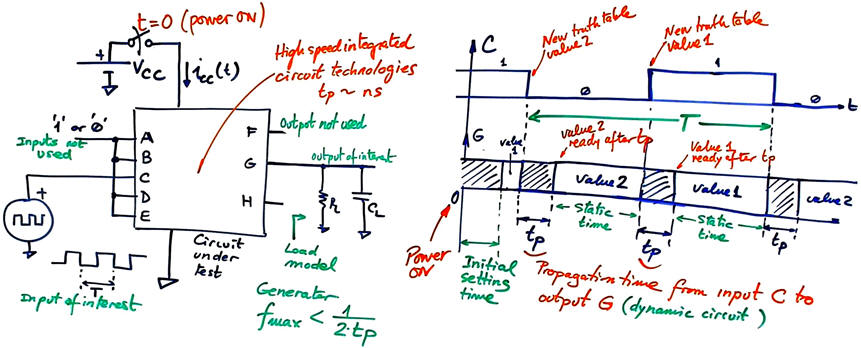 |
Fig. 1. The experiment of driving a digital circuit with a signal generator and the expected signals measured with an oscilloscope or logic analyser. In such experiment we will try to measure the signal's minimum period TMIN. or maximum frequency fMAX. The circuit calculates the truth table two times per period. |
In a similar fashion, as shown in Fig. 2, we can imagine an instrument to drive our circuit under test with vector inputs. A new data input every time T. We can measure how long does it take to set the corresponding outputs determined by the circuit's truth table.
 |
Fig. 2. The testbench for stimulating a digital circuit using vector inputs. The expected signals visualised in a logic analyser, using vertical cursors we will determine propagation times or how long does it take to calculate the truth table. |
Circuit speed is totally related to power consumption (W), therefore we aim to discuss these two concepts in the same lecture.

1.6.3.4. Current and power consumption.
Currents (pA, nA, μA, mA) and power consumption (pW, nW, μW, mW)
Powering a logic gate and connecting a switching signal. Example of CMOS_Gates.pdsprj adapting circuit structures proposed in datasheets.
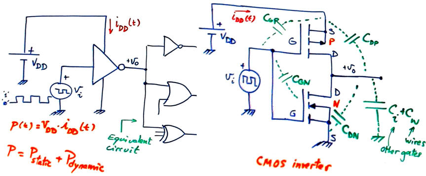 |
Fig. 3. A single logic NOT gate connected to a pulse generator and to a load composed by several other gates. To make it simple, we will consider ideal input conditions (very high Zin ) and ZL represented by a lumped load capacitor. |
Fig.4 shows a NOT transfer function and equivalent circuits in three region. This is a NOT_Gate.pdsprj where you can see how even the input protection circuit can be modelled. It only works when inputs are higher or lower than power rails VDD and GND.
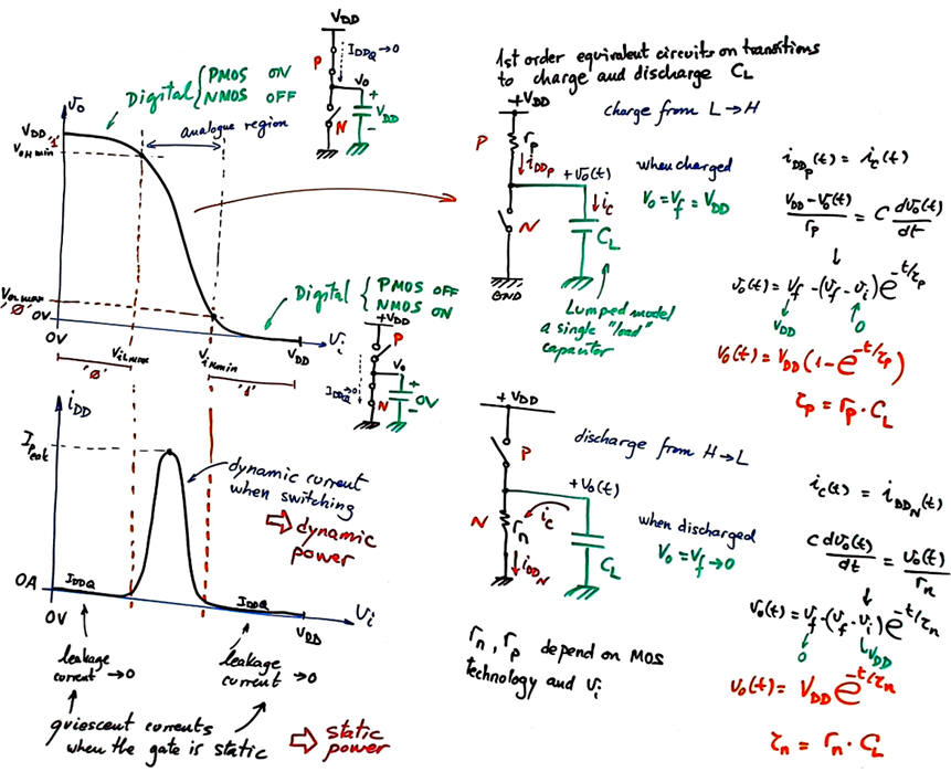 |
Fig. 4. CMOS NOT gate and its transfer function. There is a forbidden (analogue) voltage input band where the gate is transiting between logic levels. Transitions between digital levels will take time because even if there are only parasitic capacitors in the circuit, charging and discharging them cannot be done instantly. |
Therefore, the gate can be modelled using three equivalent circuits. Two static circuit with ideal switches ON and OFF, and practically zero current, meaning a very low static power consumption. And a first order equivalent circuit valid for charging and discharging CL in transitions. CL is a lumped component modelling all parasitic capacitances at output terminal.
Static power dissipation is the power consumed when the output or input is not switching (or switching at very low frequency). Normally, static power dissipation is caused by leakage current (quiescent current).
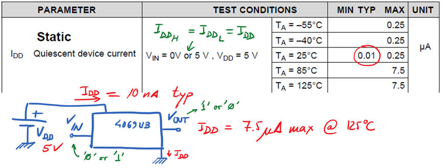
CMOS technology has very low static power consumption. Fig. 5 shows data from 4069UB sextuple NOT chip. Typical quiescent current for the device (6 NOT gates) is only 10 nA @ 25°C.
 |
|
Fig. 5. CMOS IDDQ do not changes on logic values, it is the same for Vo = VOH and VOL. |
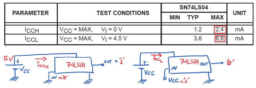
Bipolar technologies have a larger static power consumption. Fig. 6 shows data from 74LS04 sextuple NOT chip. Furthermore, quiescent current when the output is high (VOH) is different from quiescent current when output is low (VOL).
 |
|
Fig. 6. TTL-LS ICCQ depends on the output values. Datasheet shows current consumption ICCH when all (six) inputs are at '0', and ICCL when all (six) inputs are at '1'. If we imagine driving the input with a low frequency square wave (50% VOH, 50% VOL), the maximum static power consumption of a single logic gate is PS = 22.5 mW. |
Dynamic power Pdyn is the power consumed by digital circuits when processing at high speed. For instance, in CMOS technology dynamic power consumption is caused by non-negligible switching currents in transition times when charging and discharging output parasitic capacitors; transistors cannot be modelled as perfect switches with zero seconds switching times, and thus they are not ideal. Moreover, in transitions both NMOS and PMOS transistors are momentarily conducting at the same time at signal edges. The higher the frequency of operation the higher the dynamic power because transition times a preponderant factor in every period.
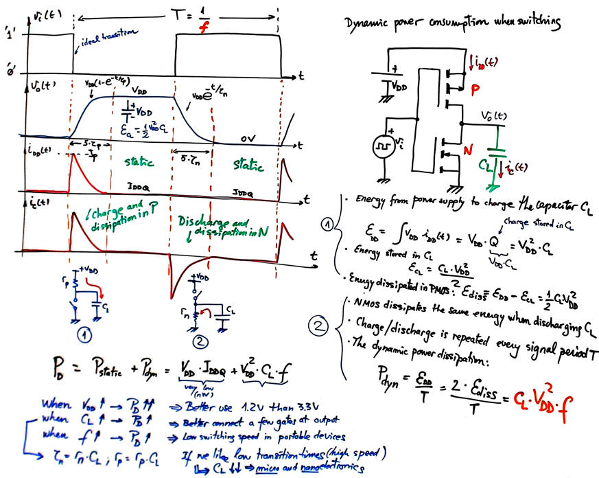 |
Fig. 7. Analysing currents in one period of signal switching. Calculating the dynamic power consumed by P-MOS and N-MOS transistors. |
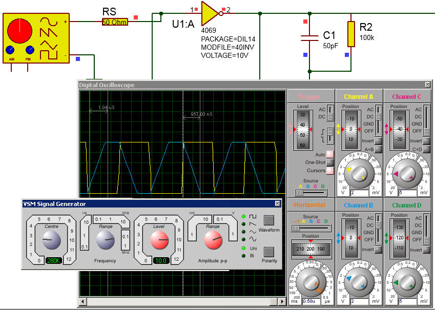
We can run Proteus simulations and represent results using CMOS_NOT_switching_LF.pdsprj. For instance, in Fig. 8. there is the circuit running at low frequencies (1 kHz) where tH and tL are predominating over transitions times. Current IDDQ will be very low, in the range of pA or nA.
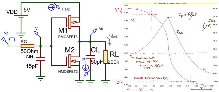 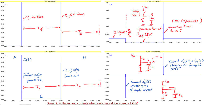 |
Fig. 8. Switching the NOT gate at low frequencies. If RL is very high, the average current value over a period is very low because static terms predominate (TH, TL >> tr, tf). Pdyn = CL · VDD^2 · f = 1.25 μW. |
In Fig. 9. there is the same circuit running at high frequencies (150 kHz) where transition times tPHL and tPLH are very long with respect the period duration. Current IDD will be very high, in the range of μA because the circuit is switching for most of the period.
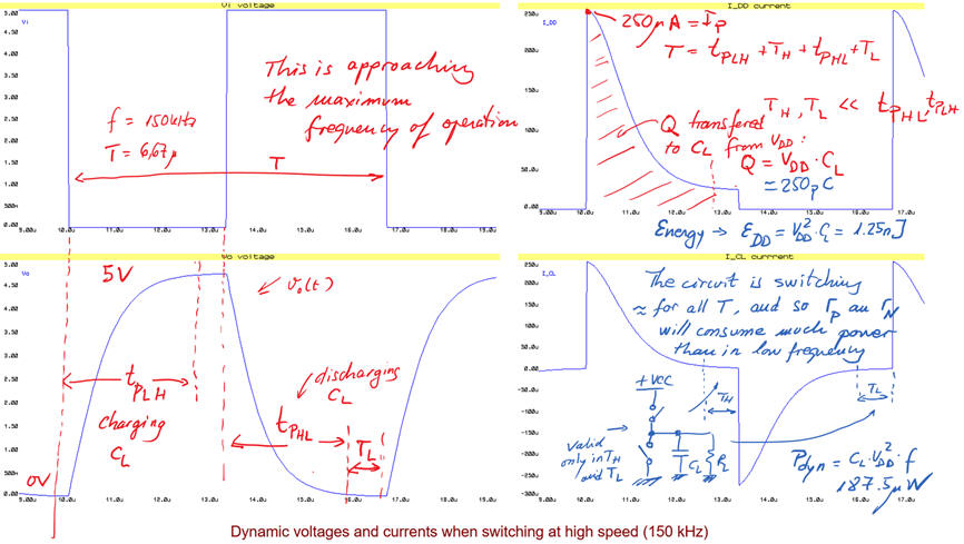 |
Fig. 9. Switching the NOT gate at high frequencies. The mean current value over a period is high because dynamic terms predominate (TH, TL << tr, tf). Pdyn = CL · VDD^2 · f = 187.5 μW |
1.6.3.5. Digital circuit propagation time, worst-case scenario: longest propagation delay
Propagation delay (~ns)
Rise and fall times describe the dynamics at the output of a logic element, and as shown in Fig. 10, the simple first order circuit for charging and discharging CL is a good approximation.
Propagation delay tP of a signal path is the time required to change the output when a change at the input is produced. It is required studying semiconductor physics to be able to relate output timing to input timing. We will simply read these parameters from datasheets because the simple first order circuit in Fig. 4 is not enough.
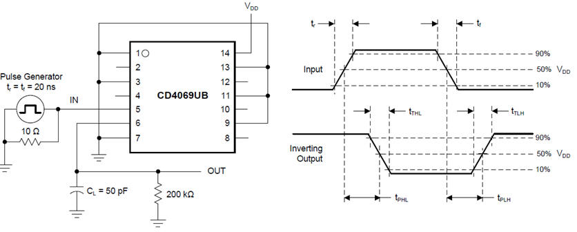 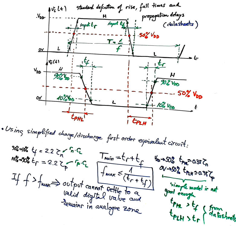 |
Fig. 10. Propagation delays, rise and fall time definitions from datasheets. We can use the simplified first order circuit in Fig. 4 to estimate these parameters. fMAX is the maximum frequency that can be applied to the circuit by a signal generator in the testbench. The circuit running at this frequency will be all dynamic. |
We better rely on datasheet data and represent propagation delay idealising the waveforms for clarity. Every technology has specific propagation delays tPHL and tPLH.
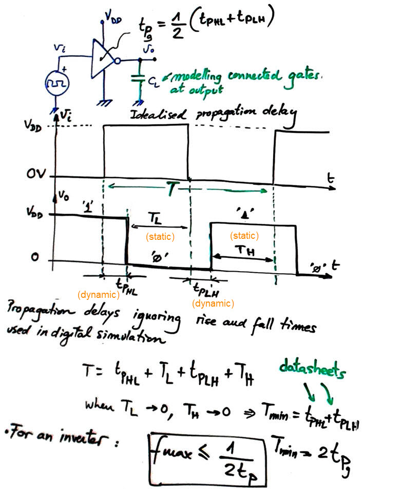 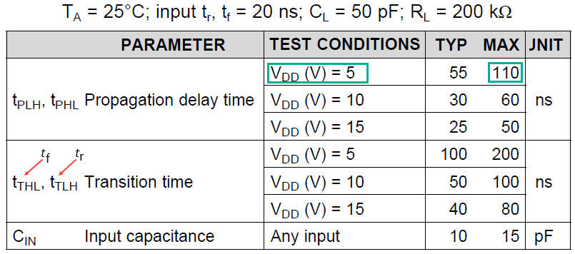 |
Fig. 11. Signals represented without considering rise and fall times, ideal signal transitions and propagation delays. Example of switching parameters from 4069UB CMOS sextuple inverter chip. Test conditions such load capacitor CL modelling loads determine typical values. Higher VDD means shorter delays but higher power consumption. |
1.6.3.6. How fast is a digital circuit calculating the truth table?
Maximum switching speed (~MHz), millions of operations per second (mops)
As shown in Fig. 9 the NOT gate cannot switch much faster than about 160 kHz, because higher than this frequency valid digital logic levels are not attained and thus Tmin = tPHL + tPLH = 2·tPg. The logic gate requires tPLH or tPHL to calculate its new truth table value. For a circuit consisting of a single gate, the frequency of the input signal generator will be fMAX = 1/(2·tPg).
A digital circuit consist of several gate levels (NGL), and each gate adds a new propagation delay (tPg) to the chain from input to output. As represented in Fig. 12, if a circuit has a number of gate levels NGL = 4, the propagation delay will be four times longer. To simplify the problem in our introductory course we will assume that (unless indicated otherwise) high-to-low tPHL and low-to-high tPLH propagation delays are identical, and also that all gates in a circuit have the same propagation time tPg. In this way we can infer the worst case scenario to calculate the circuit's propagation time (tP): the longest signal path from any input to any output.
And thus, we can estimate both, the maximum number of operations per second (or the number of times per second that the circuit is capable of solving its truth table), and also the maximum frequency fMAX of a generator that can be applied to the circuit so that it still behaves as a digital device. Frequencies higher than fMAX will generate output signals that cannot be any longer identified as digital or do not perform anymore the circuit's logic function.
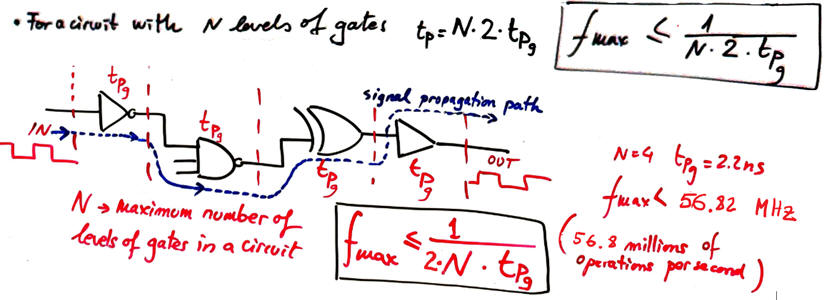 |
Fig. 12. Example circuit composed of several gate levels (NGL). |
Another example is presented in Fig. 13 for an Adder_16bit build using plan C2 and ripple carry technique. Adding all the gate levels, it contains NGL = 48.
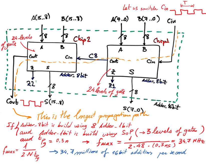 |
Fig. 13. Adder_16bit. Proteus circuit Adder_8bit.pdsprj. |
In the experiment in Fig. 14 we consider an Adder_32bit operating between two specific truth table combinations where all bits are switching. Cout is the output that will have the longest propagation delay when switching Cin with a square wave generator.
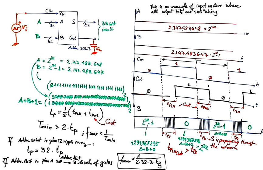 |
Fig. 14. Adder_32bit driven with specific values to switch all the output bits. |
Using this Proteus circuit, we can experiment with the Adder_32bit.pdsprj. As we can infer, its propagation delay is four times the propagation delay of the Adder_8bit because is designed simply rippling carry signals.
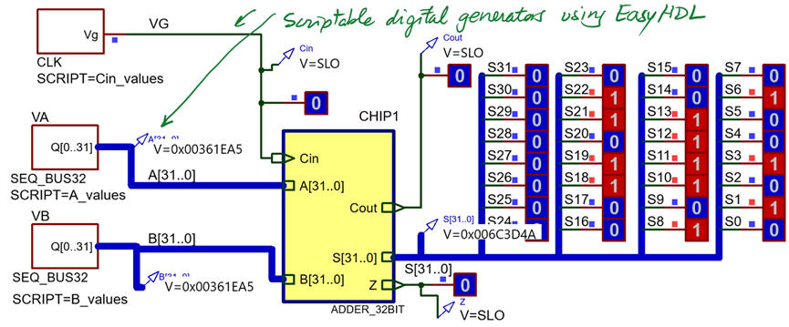 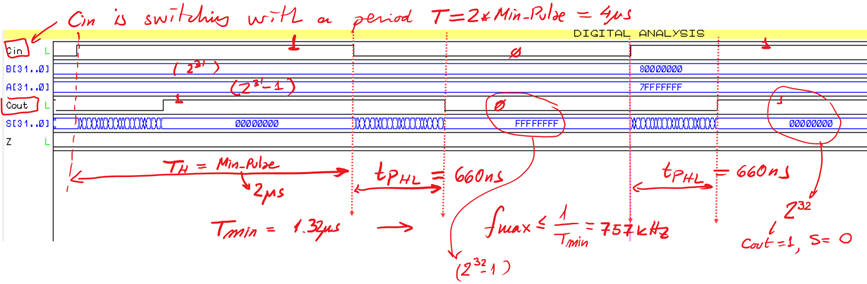 |
Fig. 15. Adder_32bit based on TTL-LS technology switching using Proteus and graphical analysis. It can perform up to 1.5 million of additions per second. |
Simulation of a CMOS inverter gate 4069 in Proteus.
 |
|
Fig.16. Example of a CMOS inverter type 4069 simulated in Proteus. |
Simulation of a TTL-LS 74LS04_inverter gate in Proteus.
Example of a simple programmable logic device sPLD solving a function. Maximum speed of operation.
Example of a CPLD electrical characteristics.
Example of a FPGA electrical characteristics.
Open collector, open drain gates, definition and how they work
Some logic gates integrated circuits have outputs with open collector or open drain so that the user can define the high digital logic level to glue or interface specific devices or adapt logic families with different voltage margins.
1.5.5. Test and verification (technology)
1.5.5.1. Gate-level simulation: propagation delay measurements
Gate-level simulation. How to measure the propagation time for a given target chip: post-synthesis model in VHDL (VHO file and its associated SDO/SDF delay file) and gate-level VHDL simulation presented in LAB 4.1.
1.5.5.2. Timing analyser spreadsheet tool: worst-case scenario, longest propagation delay
1.5.5.3. Calculating circuit's maximum speed
Thus, to summarise this lesson, two kind of experiments are possible:
(1) A circuit synthesised for two PLD's: different technologies or different vendors imply different speeds of processing (tPg). For instance an Int_Add_Subt_16bit circuit will generate different processing speeds when synthesised for an Intel or a Xilinx FPGA. Or for an Intel MAX II and for an Intel Cyclone IV.
(2) A circuit planned using different strategies (plans) synthesised for a given PLD. For instance, ripple-carry and carry-lookahead adders will have different speeds of processing. Calculate such parameters for both ripple-carry and carry lookahead 4-bit adders, compare and discuss. As usual, all the necessary files for developing and testing using gate-level simulations and timing analyser tools are in these tutorials in the corresponding sections.
1.13. Target chips: programmable logic devices (PLD)
Reviewing target chip technologies: programmable logic devices
1.13.1. sPLD (ispGAL22V10) and programmable arrays to implement logic functions
1.13.2. CPLD: complex programmable logic device
1.13.3. FPGA: field programmable gate array
Activity #1: Solve the following question:
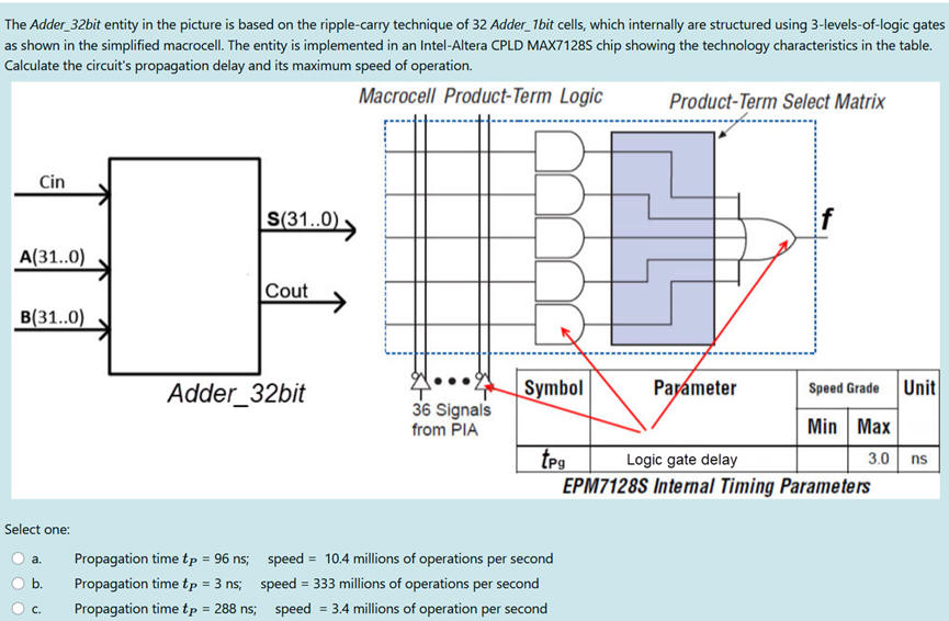
Activity #2: Solve the following question:
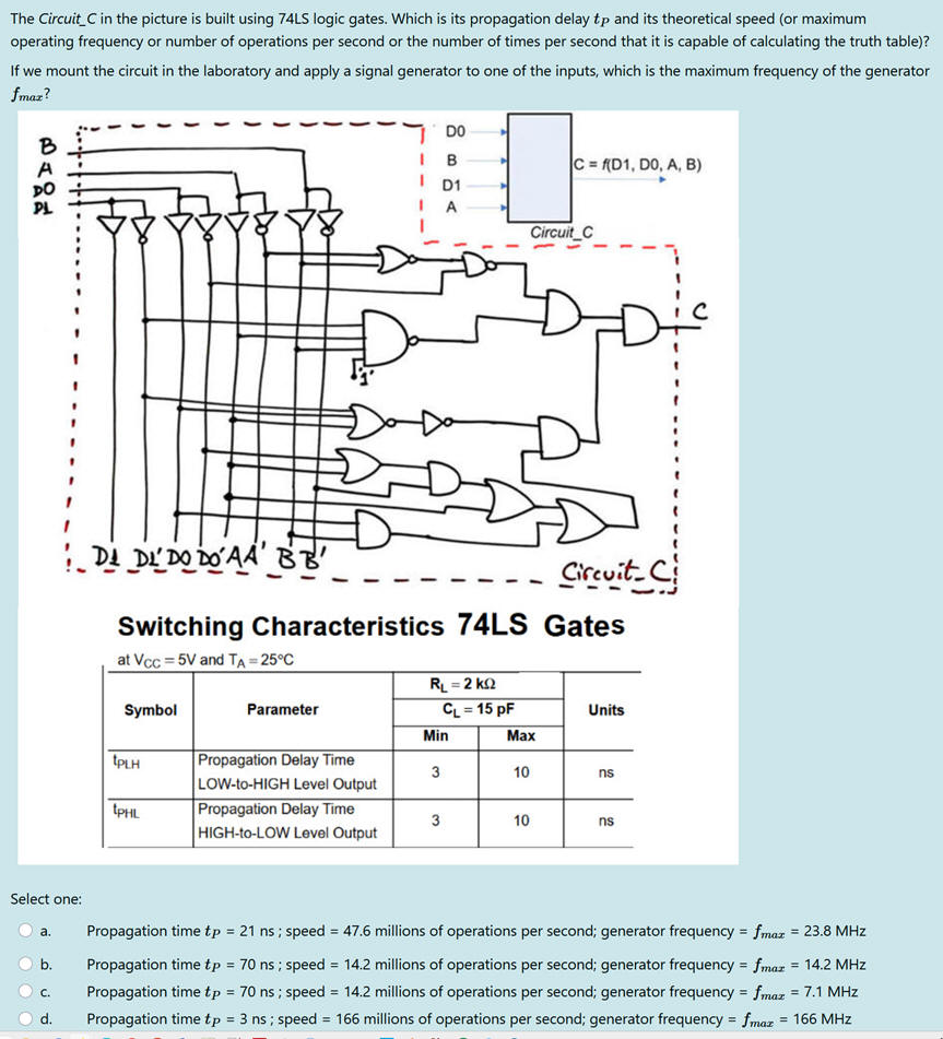
Activity #3: Determine how fast is the following circuit calculating its truth table. a) Technology LS-TTL (activity #2 above); b) technology CMOS (VDD = 5 V).
Calculate the circuit's power consumption at DC or low frequency (10 Hz) and also at the maximum frequency. We will broadly assume as an approximation that all the gates are switching.
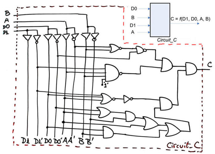
Solution ideas: From the LS_TTL datasheet we write down the maximum propagation delay of a gate tPg = 15 ns imagining all the gate with the same switching characteristics. Examining the circuit architecture we see that the longest propagation path, for example from D0 to C is NGL = 7 gate levels. Thus,

Therefore, we can drive D0 using a signal generator with a maximum frequency of

An example of Circuit_C.pdsprj testbench fixture for visualising and measuring such parameters is shown in the picture. D1 = A = B = '0', D0 is connected to a square wave TTL generator. We can use the standard load 50 pF//200 kW indicated in the datasheet.

The delay tPHL or tPLH = 105 ns is what it takes the circuit to calculate the new value of the truth table. Hence, we can order the circuit to calculate the truth table more that 9.5 millions times per second, which is indicated as mops (millions of operations per second).
Repeat the experiment for CMOS technology and compare circuit's speed.
| Home Term 26/27-Q1 Contact Products Electronic devices and companies Software Books Magazines Instruments DEE Library EETAC DEEL |

|
|
| Web activa des de 09/2001, @ F. J. Robert, Web editat amb Microsoft Expression Web 4. El contingut és un complement als materials d'estudi del curs Circuits i Sistemes Digitals disponibles al campus digital Atenea. Llicència:Reconeixement 4.0 Internacional de Creative Commons |