|
|
Bachelor's Degree in Telecommunications Systems and in Network Engineering |
|
L4.2: Arithmetic and Logic Unit (ALU) [P2-P3-P4] Multifunctional circuits for logic and arithmetic processing |
[13 Oct] |
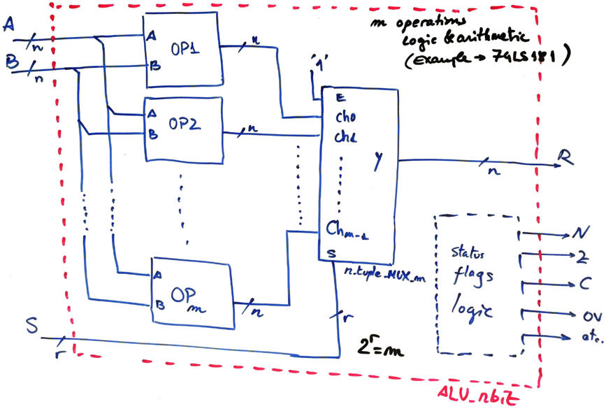
1.11. Arithmetic Logic Unit (ALU_4bit)
1.11.1. Conceptual architecture
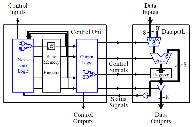
Arithmetic and logic unit architecture is modelled in this way, n-bit m operations can be selected using a multiplexer.
1.11.2. Bitwise logic operations (AND, OR, etc.)
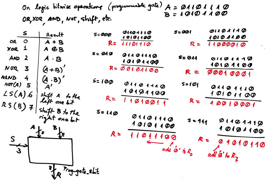
This bitwise logic operations also introduces the concept of programmable or configurable gate.
Using an ALU and in a sequence of serialised operations, several computations can be performed with input operands.
For instance, if you have to perform an 8-bit subtraction in two's complement R = A - B , you can organise this sequence of operations, saving partial results R in memory positions (data registers explained in next Chapter 2).
Algorithm to be solved: R = A - B = A + (-B) = A + 2C(B)
1) A = B ; B = x (don't care) ; R = NOT(A) (logic) --> and save partial result in Buf1
2) A = Buf1 ; B = 1 ; R = A + B (arithmetic) --> and save result again in Buf1, so that it contains now the 2C(B)
3) A = A ; B = Buf1 ; R = A + B (arithmetic) ---> Thus R = A - B
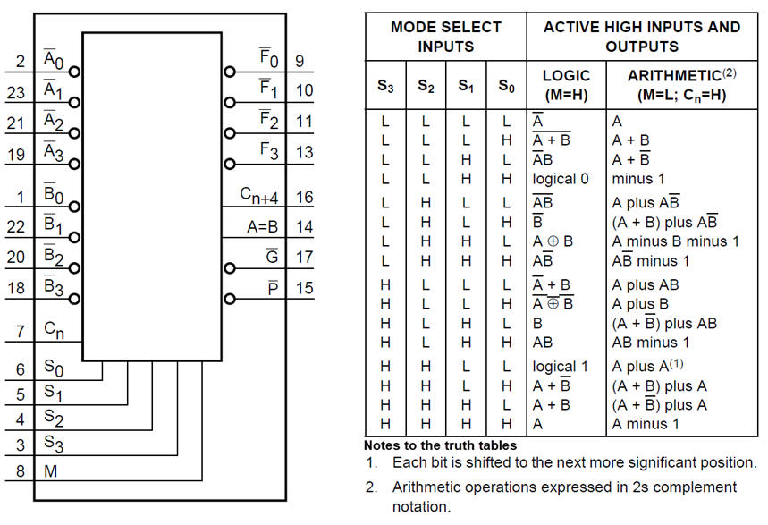
1.11.3. Commercial standard arithmetic chips in classic technologies
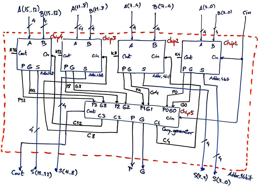
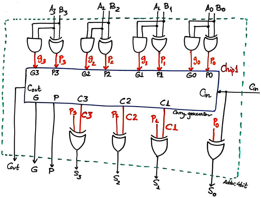
The general architecture of an arithmetic and logic unit (ALU) performing several operations in parallel and then selecting only one result. However, real chips are optimised, in the same way we studied the Int_Add_Subt_8bit in previous lecture. Example classic chip: 74LS181. And this is a carry look-ahead generator 74HCT182 to which it can be combined to speed up operations.
This is the internal block diagram on a microcontroller chip PIC18F4520, it contains an 8-bit ALU and also a hardware 8-bit multiplier.
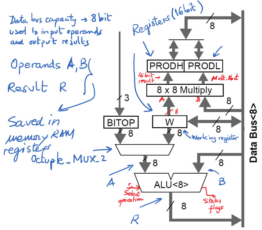
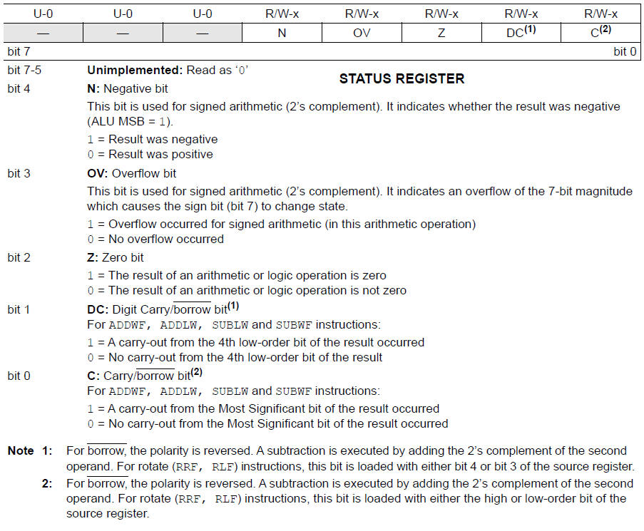
Status flags bits from ALU operations results (carry, decimal carry, sign, zero and overflow) are saved in a status register and can be used for making decisions in program flows.
There are hundreds of web pages and videos over the internet on binary arithmetic circuits. And every book on the subject has several chapters on arithmetic circuits because they are computer fundamental blocks.
 |
|
Dedicated processor representing the Arithmetic and Logic Unit (ALU) as the core of the datapath structure. Source: Hwang, E., Digital Logic and Microprocessor Design with VHDL, CL-Engineering, 2005. |
Activity #1: How fast is the circuit Adder_16bit represented in this top schematic that includes some components Adder_4bit with an internal design as show in this picture? and other combinational circuits?
Thus, discuss about the speed (mops), propagation delay time (tP), maximum frequency of operation fMAX = 1/TMIN to be applied in one of the inputs using an square wave generator, number of gate levels (NGL), and also imagine that the circuit is based in LS-TTL to find the parameter of the propagation delay of one gate (tP_1g).
Activity #2: Draw a circuit capable of performing four 10-bit operations including an OV flag.
1) A AND B
2) A XOR B
3) A - B, integer subtraction in 2C
4) A + B integer addition in 2C
Activity #3: After having completed some operations in binary to determine the circuit range and how to operate in radix-2 and two's complement, draw the plan C2 structure to invent a 6-bit selectable integer/radix-2 binary multiplier Sel_Int_mult_6bit using the component Mult_6bit represented in the figure. The Mult_6bit can be implemented using this circuit Mult_8bit that you can simulate in Proteus.
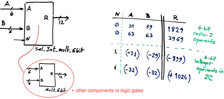
Calculate how fast is the circuit Sel_Int_mult_6bit (mops) that you have designed if we use classic CMOS technology to implement it?
Alternatively, how long will it take to run a complete VHDL testbench if we set Min_Pulse = 1.23 us? Which is the minimum value for Min_Pulse if we synthesise the circuit in target Cyclone IV FPGA chip?
| Home Term 26/27-Q1 Contact Products Electronic devices and companies Software Books Magazines Instruments DEE Library EETAC DEEL |

|
|
| Web activa des de 09/2001, @ F. J. Robert, Web editat amb Microsoft Expression Web 4. El contingut és un complement als materials d'estudi del curs Circuits i Sistemes Digitals disponibles al campus digital Atenea. Llicència:Reconeixement 4.0 Internacional de Creative Commons |