|
|
Bachelor's Degree in Telecommunications Systems and in Network Engineering |
|
L5.4: Memory chips and designing logic functions using ROM/RAM [P5] Method of ROM for solving logic functions |
[3 Nov] |
2.4. Massive digital memories
2.4.1. Symbol
- RAM (random access memory) is readable and writable
- ROM, PROM, EEPROM or Flash is only readable (it has to be pre-programmed/written previously).
ROM: read-only memory; PROM: programmable ROM; EPROM: erasable PROM; EEPROM: electrically EPROM
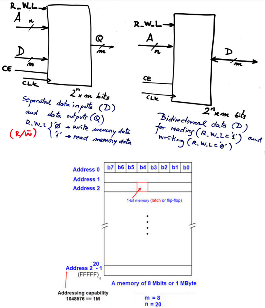 |
Fig. 1. Memory RAM_2mxn or ROM_2mxn chip symbols. |
2.4.2. General architecture
Memory structure and expansion. The idea of massive memory chips.
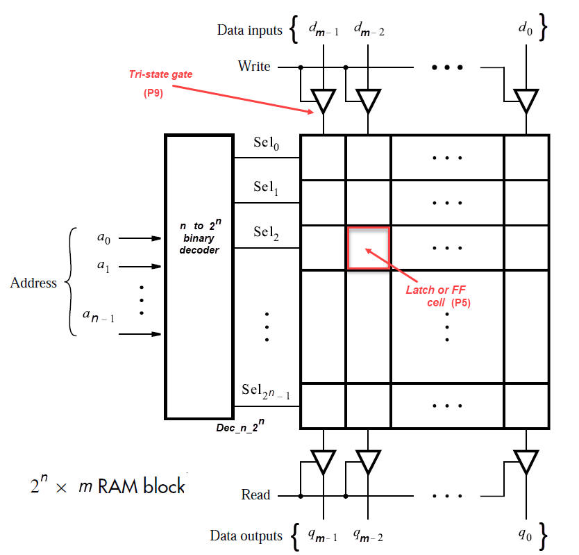 |
Fig. 2. Example of a RAM memory chip internal architecture. Using tri-state buffers, data inputs and outputs share the same cable (qi = di) because Read and Write control signals are never active at the same time (Read = Write = '1' is impossible). |
2.4.3. Tri-state gates
The tri-state gate is the last type of logic gate to be examined in our introductory CSD course. Here and now because they are used for sharing input and output ports when implementing memory chips, implementing bidirectional busses. Its functionality is represented using the model in Fig. 3 rec.
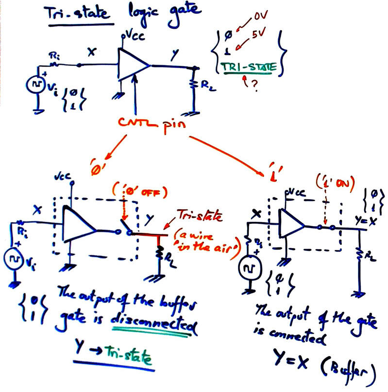 |
Fig. 3. Tri-state gate electrical model. |
Example of a tri-state gate using CMOS technology: sextuple buffer CD4003B.
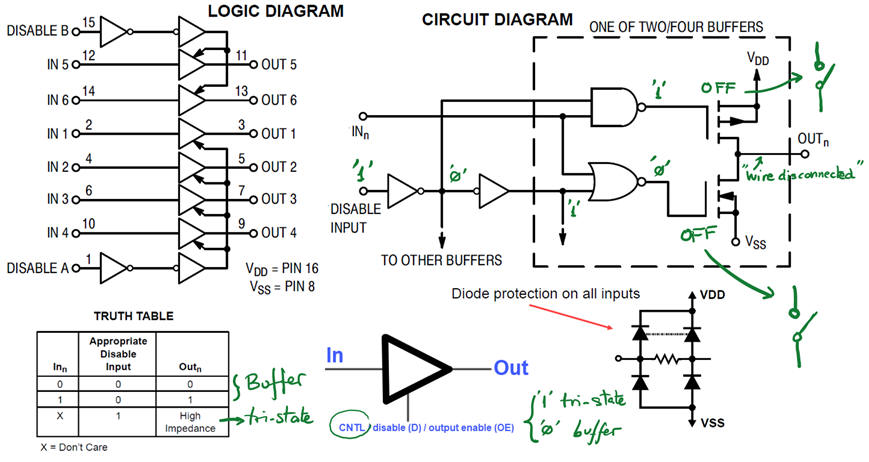 |
Fig. 4. Tri-state gate electrical model. This chip names its tri-state control input DISABLE, thus when DISABLE = '1' the gate has its output disconnected., and when DISABLE is not active ('0') the gate becomes a buffer. |
2.4.4. How to make a wire or a cable bi-directional? Bus concept
The fact that we can leave "in the air" the output of a logic gate allows connections like shown in Fig. 5 below. And this is a real technological improvement because the same wire can be configured in different time slots as input or as output. Even several chips can share the same output activating one one of them at a time. This classic 74HC245 8-bit bus transceiver is an example.
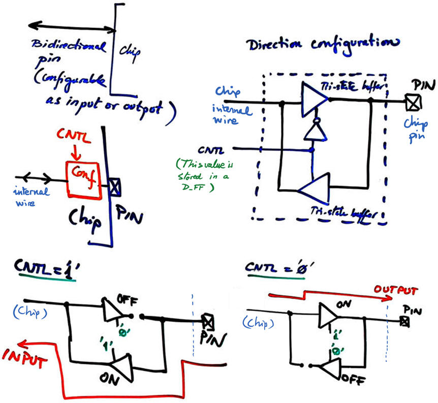 |
Fig. 5. Schematic of a bidirectional wire using tri-state gates. In this unit on I/O port pins there is more information. |
The feature of pin directionality is applied on the design of RAM or ROM memory, as shown in Fig. 6. Data inputs/outputs (IO) use the same wire for both writing and reading, but never at the same time. When reading OI is an output; when writing the memory IO wire becomes an input.
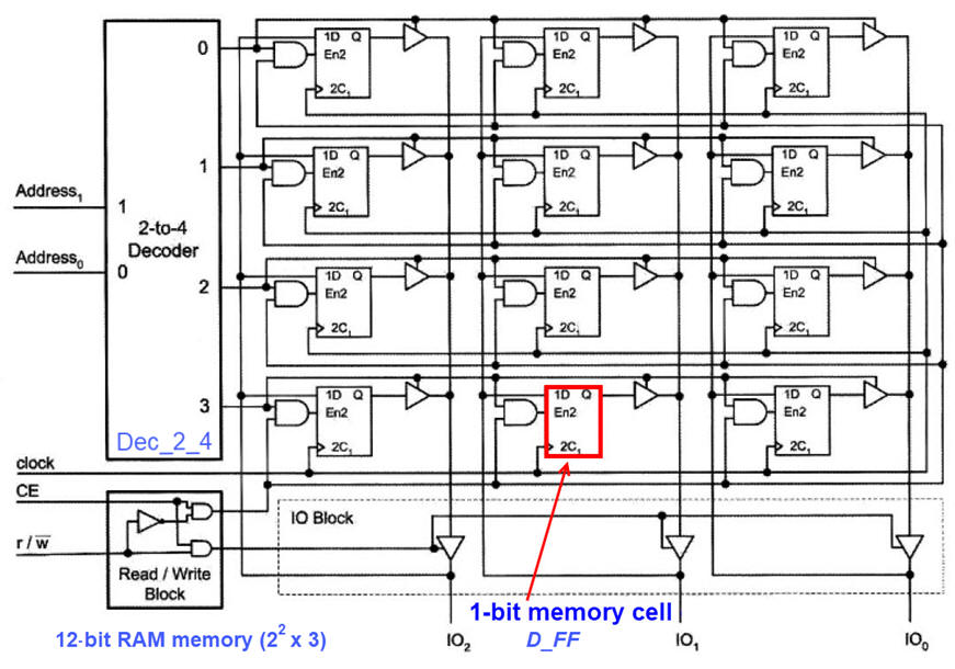 |
Fig. 6. Tri-state gates used in this schematic for implementing pins that can be both, inputs and outputs. |
Memory blocks are fundamental components for all advanced digital system (P8) and microprocessors (P9). Several kind of memory architectures are possible for a variety of applications, for example last-in first-out (LIFO) or stack, first-in first-out (FIFO). And memory chips can be expanded easily applying plan C2 to any data size (n) and addressing capability (m).
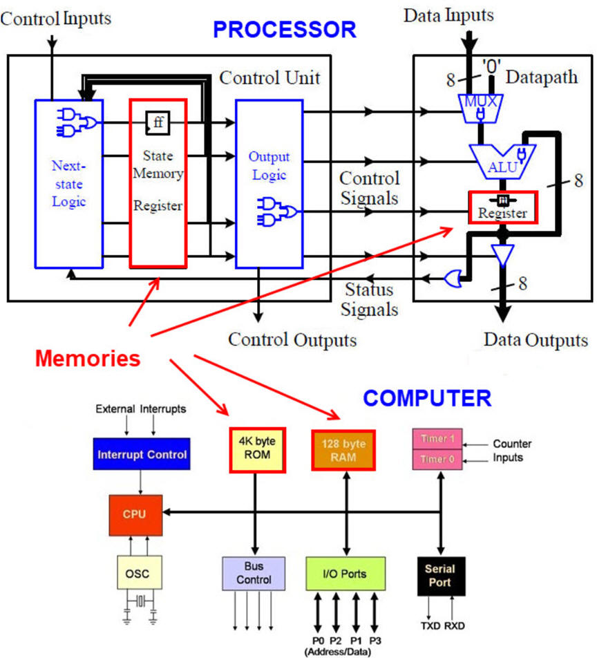 |
Fig. 7. Memories are used in all kind of digital systems. Registers are memories of m-bits in a single row. |
Memory registers, m-bit memory in a single row, are important components. For instance, Data_reg_4bit.
2.4.5. ROM: read-only memory
2.4.5.1.VHDL circuit for describing ROM memory devices.
We will use a behavioural description plan B for translating into VHDL this new component. For instance a ROM chip ROM_16x5.vhd with data cell size of n = 5 bit and 16 positions of addressable space m = 4.
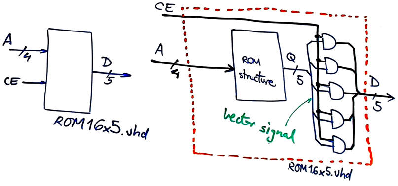 |
Fig. 8. Memories are used in all kind of digital systems. Registers are memories of n-bits in a single row. |
2.4.5.2.Method of ROM for implementing logic functions in VHDL, look-up tables (LUT)
Listed as the 14th of our plans for implementing logic functions, in CSD we will use the method of ROM/RAM memory or look-up table (LUT) for implementing combinational circuits. This is yet another plan C2 like the MoD or the MoM. This strategy is used in the fabric of FPGA logic elements for storing truth tables with a granularity of 4-input and a single output (RAM_24x1).
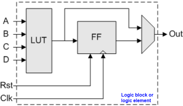 |
Fig. 9. Architecture of a logic element. |
2.4.6. (optional) RAM: random access memory
2.4.6.1. VHDL circuit RAM_2mxn (for example: RAM_16x5) and the concept of intellectual property (IP): circuits designed and optimised for a given target technology.
Advanced tutorial on RAM_8Kx8 in AMD Spartan FPGA. In this way, you can include both ROM and RAM blocks in your designs. This example can also be adapted to Intel- Altera FPGA.
Pay attention that in this example, for the first time in our introductory course, the VHDL depends on vendor libraries because the RAM is synthesised in the specific memory section of the FPGA fabric. This is the idea of IP (intellectual property) components (1), (2) related to specific technologies and vendors.
===> Using RAM memory blocks for building logic functions allow you to invent programmable circuits; every time you write RAM content, you are changing the circuit's truth table and so, the specifications of the circuit. This is the idea behind LUT block in FPGA.
2.4.6.2. Tri-state buffer in VHDL
Example of a Quad_Tri_state_buffer.vhd.
Activity #1: Design a combinational circuit such Comp_1bit using plan C2 and the the method of ROM/RAM.
Activity #2: Design a memory bank of 4 KWord (16-bit data size) using 1 KB (Kilobyte) chips and plan C2.
| Home Term 26/27-Q1 Contact Products Electronic devices and companies Software Books Magazines Instruments DEE Library EETAC DEEL |

|
|
| Web activa des de 09/2001, @ F. J. Robert, Web editat amb Microsoft Expression Web 4. El contingut és un complement als materials d'estudi del curs Circuits i Sistemes Digitals disponibles al campus digital Atenea. Llicència:Reconeixement 4.0 Internacional de Creative Commons |