|
|
Bachelor's Degree in Telecommunications Systems and in Network Engineering |
|
Lecture 6 |
L1.6. Electrical characteristics [P1] Voltage levels, '1' and '0', noise margins, power dissipation, technology |
[18 Sep] |
1.6. Standard logic gates chips and circuits
The world of digital electronic technologies is formidable and a huge industry. It is also a high-end research area. In this introductory CSD subject our aim is very simple: let us discover basic features of logic gates and programmable devices such as voltages, currents and static power consumption. Ahead in L2.4 we will discuss how to use output current for driving LED and other devices. Dynamic characteristics will be introduced at L4.3.
1.6.1. Logic families
1.6.1.1. TTL, LS-TTL, HC, HCT, etc.
 |
|
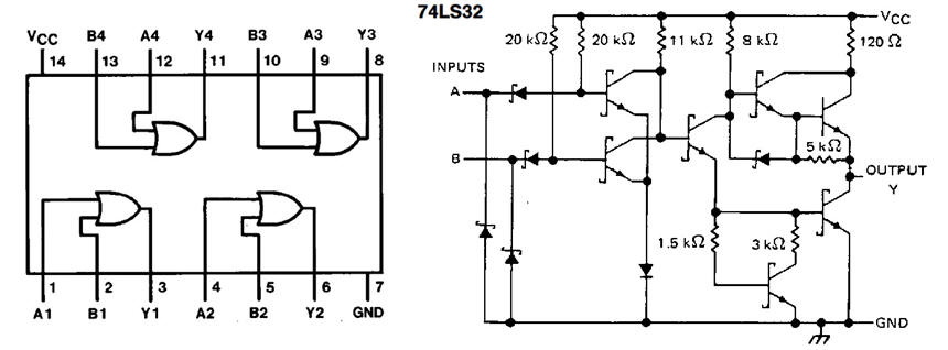
Fig. 1. Example of electronic circuit for a 2-input OR logic gate 74LS32 (LS-TTL). |
1.6.1.2. CMOS. How do NMOS/PMOS transistors work as ideal electronic switches?
 |
|
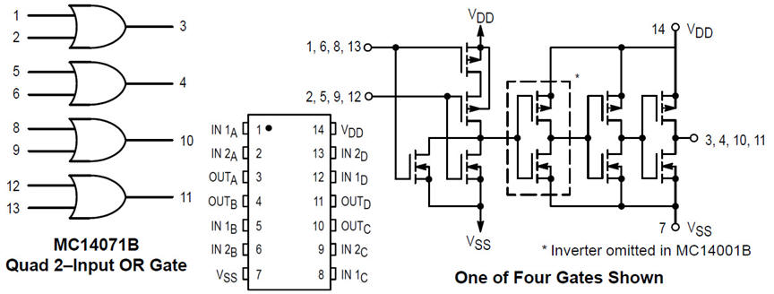
Fig. 2. Example of electronic circuit for a 2-input OR logic gate MC14071B (CMOS). |
Example of CMOS_Gates.pdsprj adapting circuit structures proposed in datasheets. This document on logic circuits from Texas Instruments is a convenient book covering these technologies.
1.6.2. Standard chip references for classic logic families
Standard logic gates and chip references. Standard symbols: traditional and ANSI. Common logic families (1), (2).
1.6.3. Electrical characteristics of logic gates
Some basic ideas to start on voltage values, noise margins, power rails, transfer VO = f(VI) curve, etc.
1.6.3.1. Voltage levels. What voltage range is interpreted as '0' and as '1'? VOHMIN, VOLMAX, VIHMIN, VILMAX
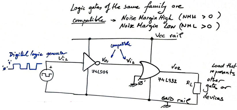
1.6.3.2. Noise margin high (NMH), noise margin low (NML), logic family compatibility
Voltages and logic levels rec. Which voltages are interpreted as a '0' and a '1' at the input or at the output of a logic gate?
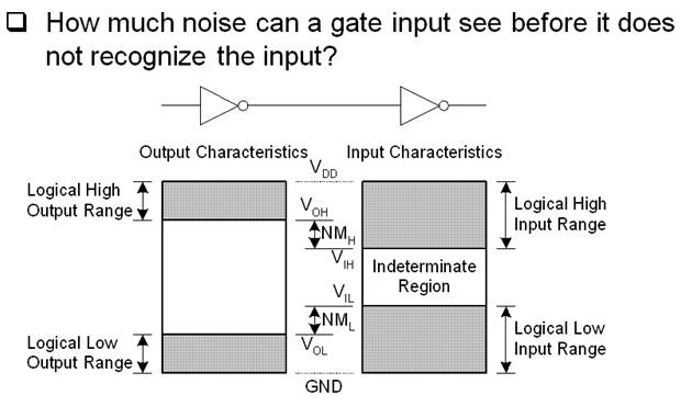 |
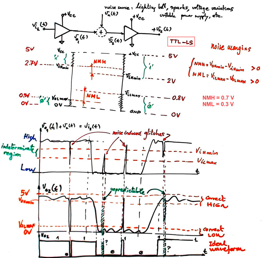
Fig. 3. Definition of the high and low noise margins (source ref.) Technology 74LS (for instance, chip 74LS04) or CMOS 4069. If the added noise is high, digital voltages can be severally altered and misinterpreted by logic gates, generating false digital signals or unpredictable results. Digital signals must be kept varying in the corresponding margins. |
  |
|
The idea of noise affecting negatively a digital circuit is exemplified in this slide from Doulos on designing safe FSM (P6, chapter II content).
You can run this Circuit in Proteus to get an idea on voltage levels, currents, power consumption and logic values.
1.6.3.3. Input-output transfer characteristic VO = f(VI)
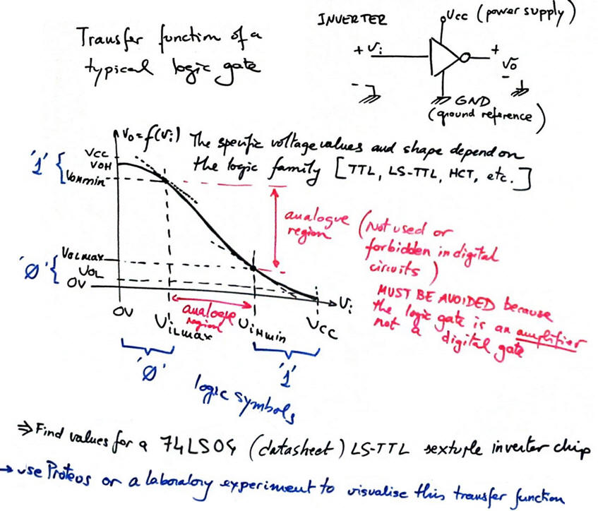 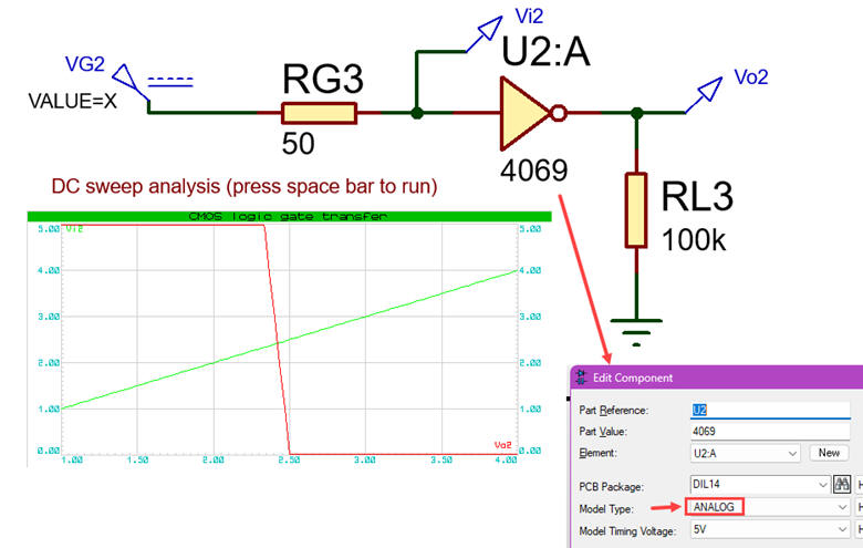 |
Fig. 4. Input-output characteristics of a logic gate. Experimenting a DC sweep using a CMOS 4069 inverter ("Logic_gate_transfer.pdsprj"). |
Use the Proteus simulator to obtain the curve of a classic 74LS04 or 4069UB logic gate.
Other electrical characteristics not considered in Fig 3 such as switching times and propagation delays are explained in lecture L4.3.
1.6.4. Input push-buttons and switches to generate '1' and '0'
1.6.4.1. Active-high button circuit
1.6.4.2. Active-low button circuit
How to connect push-buttons and switches to chip inputs to generate '1' and '0'? rec.
This is "Circuit_W.pdsprj" to play with buttons and switches in Proteus.
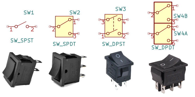
Industry standard symbols for switches. SW1: single-pole, single-throw (SPST) switch. SW2: single-pole, double-throw (SPDT) switch capable of routing current to one of two paths. SW3: double-pole, single-throw (DPST) device capable of simultaneously turning on two circuits. SW4: double-pole, double-throw (DPDT) switch.
 |
|
Fig. 5. Four types of mechanical switches modelled in KiCad. |
Activity #1: Play this "Circuit_W.pdsprj" in Proteus. Draw your circuits and annotate your results in paper.
(a) Generate high and low input digital voltage levels using both SPST and SPDT switches.
(b) Measure the current a the LS-TTL 74LS04 inverter input.
(c) Measure the current at the CMOS 4069 inverter input.
(d) Find the voltage margins and compare them with datasheet information.
(e) Sweep the input voltage from 0 V to 5 V ("Logic_gate_transfer.pdsprj") and draw the VO = f(VI) transfer characteristic for a given logic gate.
Activity #2: Compare power supplies, digital voltages, input and output currents, noise margins and transfer curves and pin compatibility of two logic families like classic CMOS and HCT-TTL. Use for instance two XOR2 chips: (1) CD4070B, (2) 74HCT86. For which logic family we can consider a negligible input current?

Activity #3: Analyse and explain how these two CMOS circuits work and deduce their truth table.

| Home Term 26/27-Q1 Contact Products Electronic devices and companies Software Books Magazines Instruments DEE Library EETAC DEEL |

|
|
| Web activa des de 09/2001, @ F. J. Robert, Web editat amb Microsoft Expression Web 4. El contingut és un complement als materials d'estudi del curs Circuits i Sistemes Digitals disponibles al campus digital Atenea. Llicència:Reconeixement 4.0 Internacional de Creative Commons |