|
|
Bachelor's Degree in Telecommunications Systems and in Network Engineering |
|
P10: FSM in C language (software FSM), external interrupts |
| Resources in lectures and labs: | L10.1, Lab10, L10.2 | Project | objectives |
Highlighted project: 4-bit serial transmitter
Design phases ==> #1: Serial_TX ==> #2: Serial_TX_LCD ==> #3: Serial_TX_LCD_TMR0 ==> #4: Serial_TX_LCD_TMR2
| 1. Specifications | Planning | Dev. & test | Prototype | Report |
Design phase #1: Let us design a simplified 2-wire (Serial_out - GND) asynchronous data transmitter based on a μC for sending a nibble (4-bits) of data to another computer or device. The symbol is represented in Fig. 1. Asynchronous transmissions based on Shift_Reg_4bits devices were studied in the USART tutorial (rec. part 1).
The target chip is the PIC18F46K22. We will program the application in C language using our FSM style.
In a first step #1 we can consider this simple transmission format once the start-transmission (ST) rising edge is detected by means of an interrupt. The output Serial_out is held high when idle (marking). start bit ('0'); Data_in(0), Data_in(1), Data_in(2), Data_in(3); stop bit ('1'). Additionally, while transmitting the stop bit, an end-of-transmission EoT pulse is generated to indicate that the transmitter has ended the process.
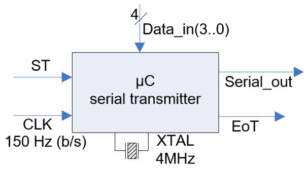 |
Fig 1. Symbol for the 4-bit serial transmitter. |
Fig. 2 shows an example of timing diagram to start transmitting data when the ST pulse is detected.
 |
| Fig 2. Example of a section of a timing diagram where it can be seen how Data_in is read and right shifted to the single wire Serial_out. |
Serial transmission (TX) and reception (RX) is used in every electronic equipment. For instance, Fig. 3 shows two examples:(a) the PC computer COM serial port and its options to choose transmission parameters; (b) the communication between ECU (electronic control units) in modern autonomous vehicles.
 a) b) 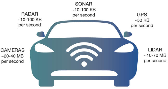 |
|
Fig 3. a) Example of the PC COM port configuration parameters for enabling asynchronous communication. This standard port can be emulated by Bluetooth or USB adapters. b) Autonomous vehicles generate huge amounts of data to be transmitted from and to high-speed digital subsystems. Reference: Keysight white paper: "High-Speed Digital Design Success Demands A Modern Workflow" (pdf). |
Logically, we can enhance our simple transmitter in successive design steps to implement for instance all the options available in the conventional COM PC port. In a next step #2 we can add the odd/even parity bit and transmit a configurable numbers of bits.
Furthermore, we can design the receiver Serial_RX that complements this asynchronous transmitter.
The idea that we have in mind in this Chapter 3 on designing software FSM is very well explained in this white paper from the microcomputers company ARM.
Other design tutorials and assignments.
| Specifications | 2. Planning | Dev. & test | Prototype | Report |
A) Planning hardware
The electronic circuit sketch is shown in Fig. 4. Some μC port pins are selected to be inputs and outputs, external interrupt INT1 is used to detect ST active edge event (falling or rising signal transition) to start sequencing the transmission. External interrupt INT0 will detect an active edge from the external CLK to be able to serialise one bit per period. The key concept in this application is detecting signal edges using interrupts. CLK interrupt can be both, enabled all time or instead, better only after start transmission edge is detected.
 |
| Fig. 4. Hardware used in this application. The 2-wire serial output cable can be simulated using a resistor R0 = 10 kΩ. The PIC18F46K22 has three port pins (RB0, RB1 and RB2) able to generate external interrupts (INT0, INT1 and INT2) when detecting signal edges (the active rising or falling transition is configurable). |
B) Planning software
The general idea is represented in Fig. 5 (rec. part 2). The concepts of CC1 and CC2 combinational circuits inherited from Chapter 2 have the same meaning, we will implement this logic using software routines.
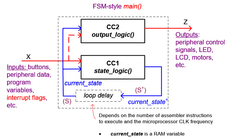 |
| Fig. 5. Software organisation used in this application. Because the current state is saved in a RAM memory position (var_current_state) and updated every main loop cycle, there is no need for the next state variable as it was the case in Chapter 2 where the state register were implemented in D_FF. |
And even a clearer flowchart reorientation of the software organisation in Fig.6 below.
 |
| Fig. 6. General interrupt-driven FSM-style program organisation (Visio). |
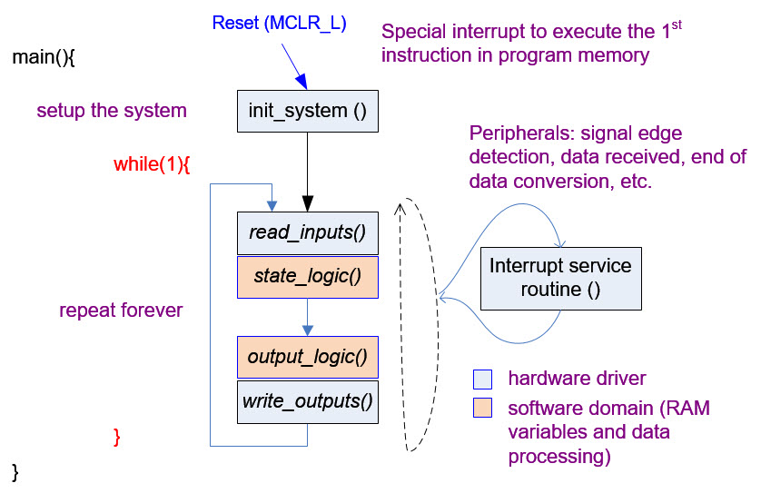
Therefore, it is possible to think in terms of a kind of hardware/software diagram as shown in Fig. 7. The idea of implementing a "FSM in software": state and output logic connected to RAM variables and additional functions related to hardware (drivers) to read and write external pins. The diagram also includes the interrupt logic hardware capable of triggering the jump from the main program execution to the interrupt service routine (ISR).
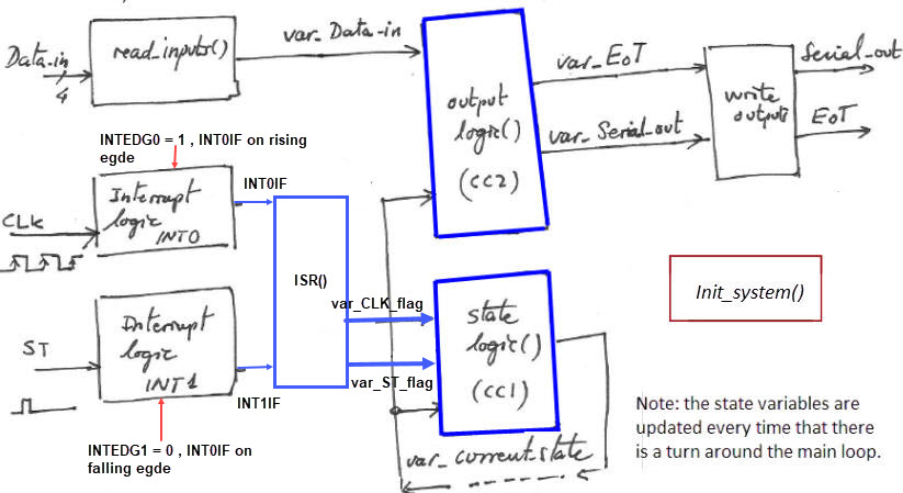 |
Fig. 7. This diagram connects in a convenient way the hardware section and the software functions for better understanding the idea of programming FSM. |
Draw the state diagram, so that the sequence represented in Fig. 2 can be generated after having detected an ST edge.
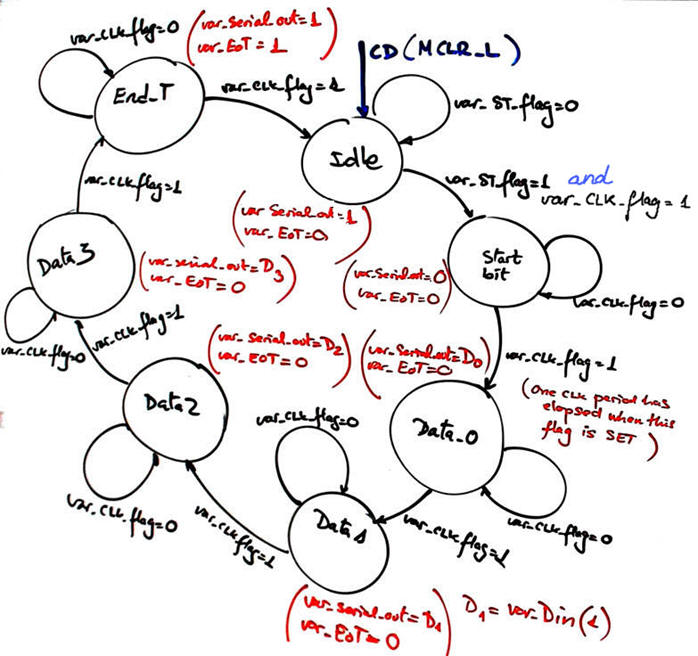 |
Fig. 8. Proposed state diagram. Be aware that all the signals represented are RAM memory variables, for instance, CLK pin is now the var_CLK_flag. When the ST button active rising edge is detected, the FSM needs six CLK periods to complete the transmission and to go back to idle state to wait for the next ST pulse. |
In Fig. 9 there is the representation of the RAM memory required in this project. At our introductory level, memory positions are not optimised in any way. Our main goal is clarity and simplicity, and thus, we like to save each signal in a different memory position zeroing all the unused bits.
Another convention to make it simple is to code FSM states in a RAM byte variable named var_current_state. Let us use ASCII capital letters to facilitate interactive debugging using the watch window. Remember that state encoding was proposed in Chapter 2 as an option to choose between several codes: sequential, Johnson, one-hot, Gray, etc.
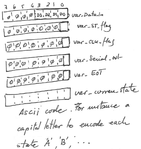 |
Fig. 9. We will use six bytes of RAM to store the variables. |
Draw the main ideas of init_system(). Configure input and output pins. Consider as well interrupts configuration.
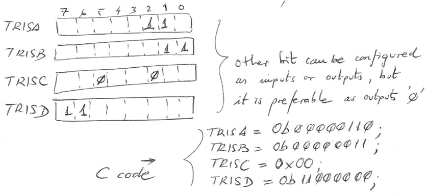 |
Fig. 10. Example of TRIS configuration. |
Draw the flowchart of read_inputs(). Basic function to poll input voltages as in L9.3.
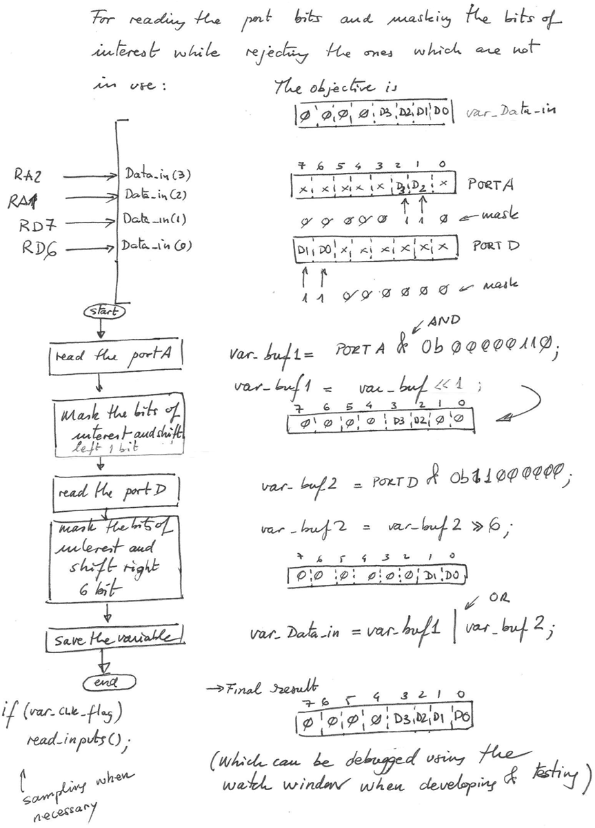 |
Fig. 11. Reading inputs ideas. |
Draw the flowchart of write_outputs(). Basic function to write pin voltages as in L9.4.
 |
Fig. 12. Example on how to write output pins. |
Infer how to organise the interrupt service routine ISR() to handle edge detections. Any time that an interrupt occurs the main program execution stops, all the registers, flags and environment is saved at the stack memory, and the the program counter jumps to the interrupt vector where is written the ISR() code. When returning from interrupt restores the environment is restored and the program counter continues executing main loop instructions.
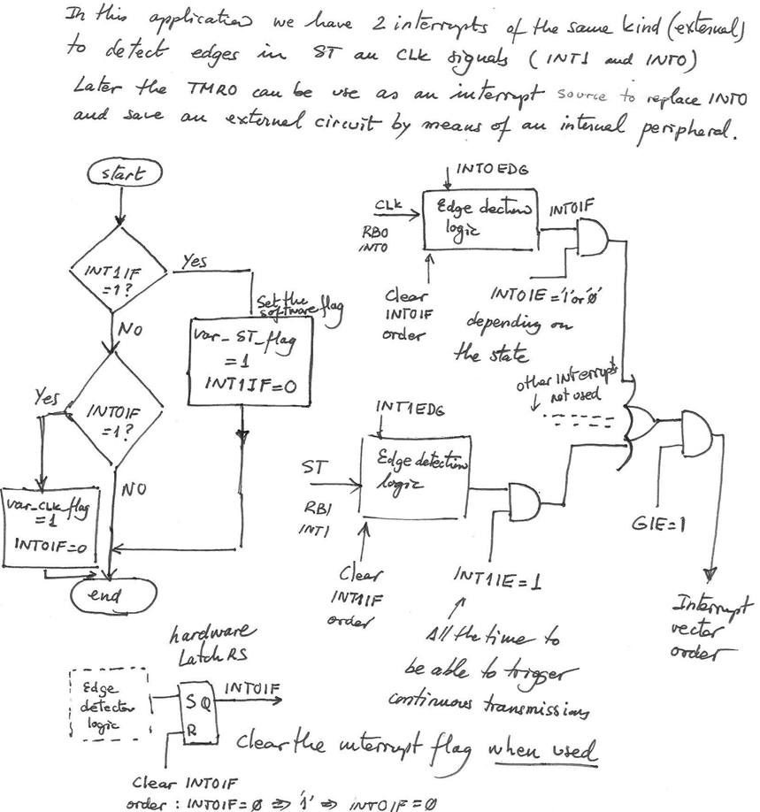 |
Fig. 13. Ideas on how to organise the ISR. |
And now, it is necessary to discuss how to transfer all the state transitions into a truth table. Draw state_logic() truth table and follow interpreting it as in plan B, in a behavioural way.
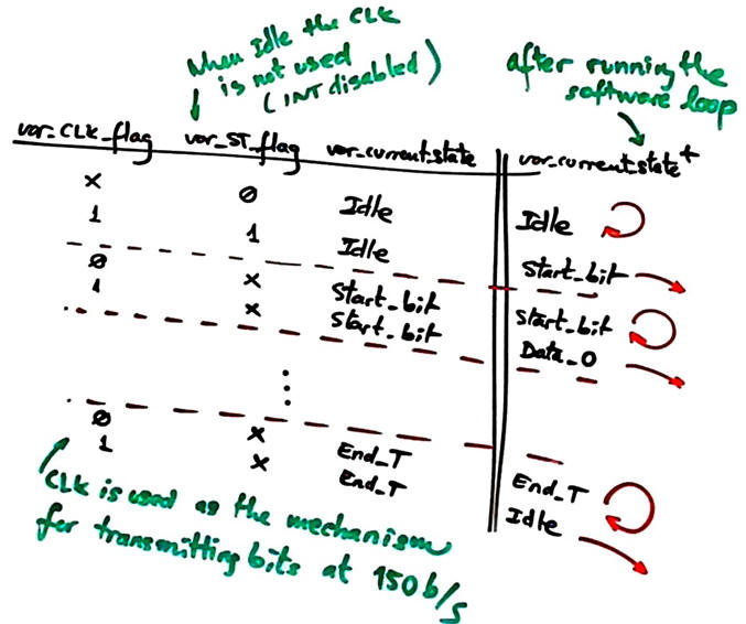 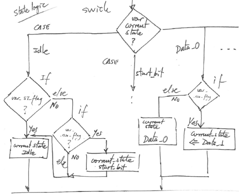 |
Fig. 14. Truth table for state_logic() function and its flow chart interpretation. Now it is straightforward to identify C statements. |
Draw output_logic() truth table. Finally, what is left to finish this project planning is the same idea but for the outputs: how to translate all the outputs in parenthesis in the state diagram into a truth able and its equivalent flowchart? This ideas are presented in Fig. 15. A Moore FSM makes it simpler than a Mealy FSM: all the outputs are perfectly defined for each state.
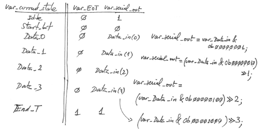  |
Fig. 15. Truth table for output_logic() function and its behavioural interpretation flowchart |
Organise a MPLABX - XC8 IDE project targeting a PIC18F46K22 at location:
C:\CSD\P10\Serial_TX\(files)
| Specifications | Planning | 3. Dev. & 4. test | Prototype | Report |
A) Developing hardware
Electronic circuit and C source code. Running simulations and debugging (rec. part 3).
This is a file "Serial_TX.pdsprj" containing the circuit represented in Fig. 16. Be aware that ST and CLK inputs must be connected to external interrupts like INT1 (RB1) and INT0 (RB0).
 |
| Fig. 16. The proposed circuit running the final executable "*.cof" to be able to debug errors and step by step mode. |
B) Developing software
Our planning ideas in previous section are translated to this C source file "Serial_TX.c". Add the "config.h" header to your project.
Run the microcontroller's IDE to develop and compile the C code to obtain executable files. This is the full project containing the executable files "Serial_TX.zip"·
Set the project name and location indicated in Fig. 17.
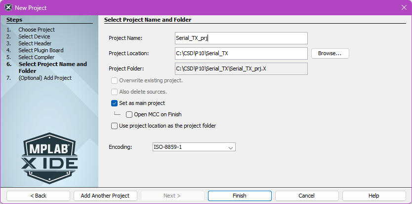 |
Fig. 17. Project location and name. |
C) Step-by-step testing
Fig. 18 shows the debugging environment running in Proteus. You can track RAM variable values in the watch window and execute the program step by step. You can also use break points to stop the execution at a given instruction. This feature is particularly useful for following interrupts. Remember that development and testing must be carried out step by step, one feature at a time.
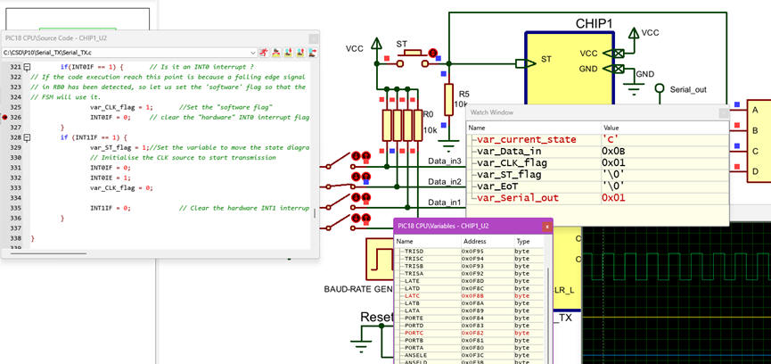 |
Fig. 18. Executing the program code using breakpoints. |
Instrumentation can be used to display transmitted waveforms. You may like to replace the ST button by a pulse generator (for instance 0V-5V, T = 1.5 s, pulse duration = 20 ms).
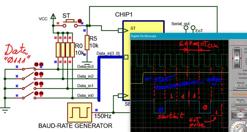 |
Fig. 19. Circuit running in Proteus. |
Example of oscilloscope measurements triggering the instrument on the ST rising edge.
 |
Fig. 20. Waveforms captured in Proteus showing the transmission of the four bytes once the start bit is low. |
NOTE: Do not print the picture with black background in Fig. 20. Configure and change colours as indicated in Fig. 21 to save ink when printing and annotating pictures for your reports.
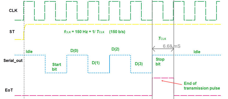 |
Fig. 21. Project location and name. |
Activities for experimenting:
- Check that the machine is always under control running through the enumerated states (watch window --> var_current_state).
- Measure the duration of a transmitted bit using breakpoints.
- Check that var_ST_flag has the right values when start transmission button is pressed.
- Measure how long is the CLK interrupt enabled.
- Calculate how fast is the execution of the main loop.
- How long does it take to execute the ISR()?
| Specifications | Planning | Dev. & Test | 5. Prototype | Report |
Example 1: Board CSD_PICstick . Target microcontroller: PIC18F46K22. Tools: MPLAB X + XC8 + Proteus + VB8012 compact instrumentation. A complementary project is the design of the serial receiver Serial_RX.
You can also develop a full transmitter and receiver unit USART.
| Specifications | Planning | Dev. & Test | Prototype | 6. Report |
Follow this rubric for writing reports.
| Home Term 26/27-Q1 Contact Products Electronic devices and companies Software Books Magazines Instruments DEE Library EETAC DEEL |

|
|
| Web activa des de 09/2001, @ F. J. Robert, Web editat amb Microsoft Expression Web 4. El contingut és un complement als materials d'estudi del curs Circuits i Sistemes Digitals disponibles al campus digital Atenea. Llicència:Reconeixement 4.0 Internacional de Creative Commons |