|
|
Bachelor's Degree in Telecommunications Systems and in Network Engineering |
|
|
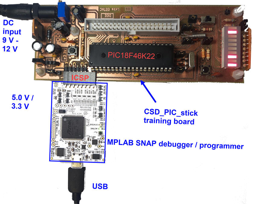
CSD_PICstick development board |
||
We can implement prototypes for simple circuits based on microcontrollers using standard commercial boards such as EXPLORER8 , older PICDEM2. or any other legacy similar board. However, it is interesting and educational to design a custom training board for solving our introductory CSD lab exercises. This is the purpose of the CSD_PICstick proposed in this unit.
| 1. Specifications | Planning | Developing | Testing | Report |
Let us conceive a simple training board containing these features:
- 40 pin and 28 pin sockets for mC such PIC18F46K22 and PIC18F26K22.
- Reset push-button (MCLR_L).
- Primary 8 MHz (OSC1, OSC2) and secondary 32.768 kHz (T1OSI, T1OSO) XTAL oscillators.
- Connector ICSP for chip programming and debugging using commercial MPLAB SNAP device, PICkit5 or ICD5.
- Unregulated DC input VIN from 8 V to 15V. Power LED indicator.
- Selectable PIC voltage: VCC = +5V or +3.3V.
- 8 LED to represent binary codes (or a 10-LED bar).
- Active-low push-button at RB0/INT0.
- Switch at RA4.
- Analogue input at RA0/AN0.
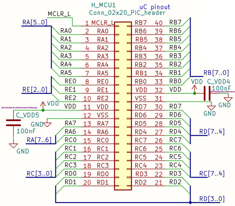
- 20x2 header connector with all microcontroller pinning.
 |
| Fig. 1. The CSD_PICstick idea. Jumpers will be used to connect or disconnect some circuits. The 40-pin expansion connector allows the insertion of any daughter board. |
| Specifications | 2. Planning | Developing | Testing | Report |
In this section we will imagine the hardware circuit and where all inputs and outputs are connected. We will leave the schematic ready to be captured as a KiCad project.
 |
| Fig. 2. Ideas on the schematic. We will use 40-pin and also 28-pin mC sockets. |
Power adapter
You can use the laboratory power supply like VB8012 or a cheap standard unregulated AC 220V to DC 9V @ 1A adapter to power the CSD_PICstick with +5V or +3.3V depending on the target mC.
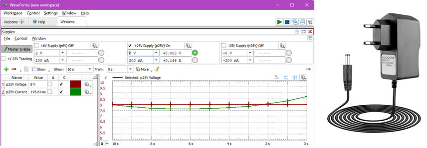 |
| Fig. 3. DC power supply or AC-DC power adapter. |
| Specifications | Planning | 3. Developing | Testing | Report |
NOTE on coding styles: In CSD, including this unit on the CSD_PICstick, we propose to program in C at the simplest register-level or bare-metal. However, for advanced users or in case you like to continue developing these applications in a professional fashion, we have added a unit with several examples to start with the MPLAB Code Configurator MCC Melody.
Before designing the PCB, we can check whether the basic idea of the board and its inputs, outputs and oscillators works correctly solving as usual a given example in Proteus divided in several consecutives phases. Full detail on how to plan and install a FSM in a µC is presented in P10 (phase #1), P11 (phase #2), and P12 (phase #3). For instance:
(A series of design phases to check the circuit: phase #1, phase #2, phase#3, phase #4)
(1) Design phase #1: Counter_BCD_1digit. Let us start solving the same Counter_BCD_1digit as a FSM using plan X proposed in LAB10 targeting a PIC18F46K22.
Project location to replicate this LAB10 first tutorial:
C:\CSD\CSD_PICstick\Counter_BCD_1digit\
 |
| Fig. 4. Counter_BCD_1digit captured and running in Proteus. We validate switches, push-buttons and LED. |
(A series of design phases to check the circuit: phase #1, phase #2, phase#3, phase #4)
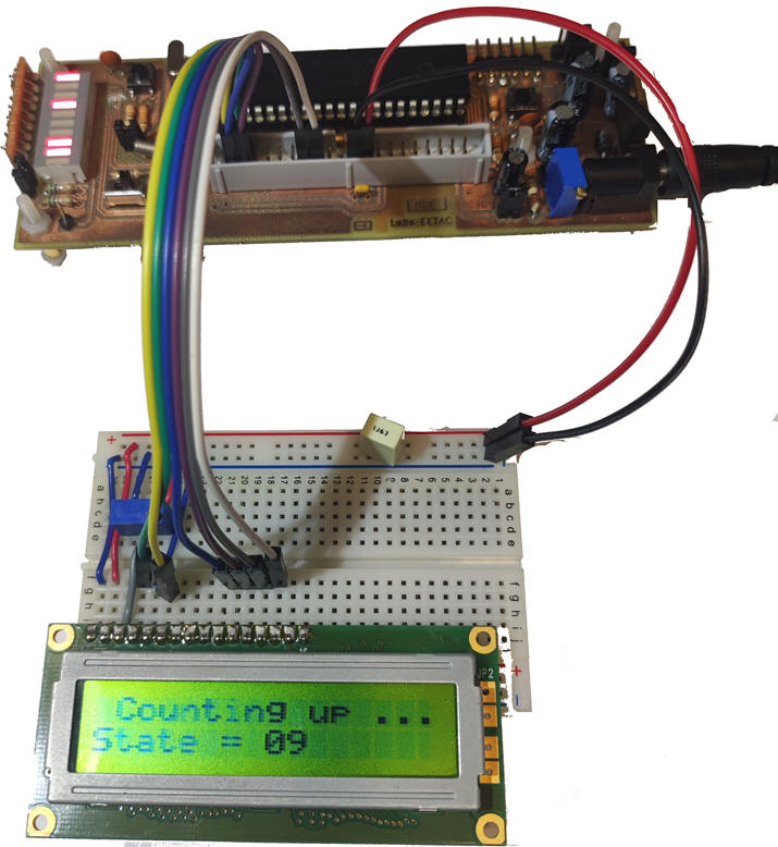
(2) Design phase #2: Counter_BCD_1digit_LCD. Let us add an LCD to the circuit using the 40-pin connector header.
Project location to replicate this tutorial:
C:\CSD\CSD_PICstick\Counter_BCD_1digit_LCD\
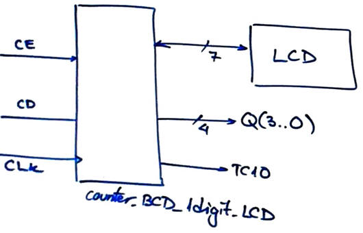 |
| Fig. 5. Counter_BCD_1digit_LCD using 6 pins to interface the LCD peripheral. |
(A series of design phases to check the circuit: phase #1, phase #2, phase#3, phase #4)
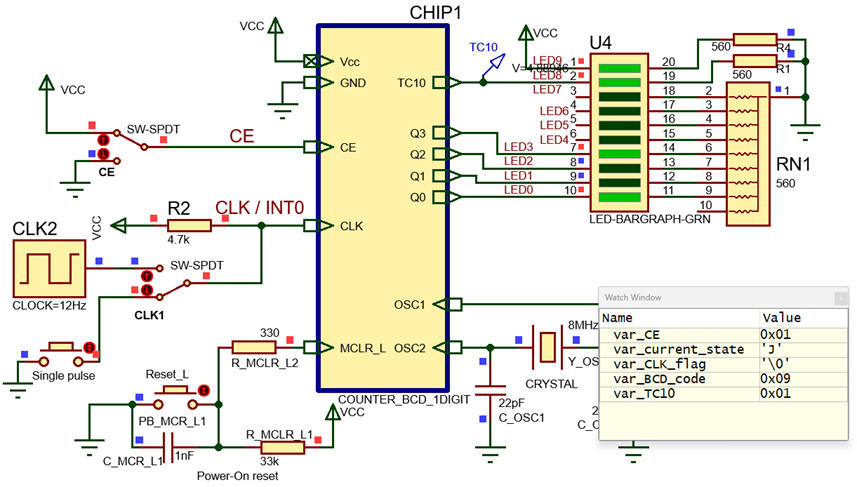
(3) Design phase #3: Counter_BCD_1digit_LCD_TMR1. In order to check that the secondary oscillator SOSC at 32.768 kHz operates correctly, we can replace the external CLK or push-button by the internal TMR1 running as timer to generate the var_CLK_flag when TMR1 overflows. Timing period TP can be selected using the free push-button as a switch Sel_freq. For instance: 1 s (1 Hz) or 83.33 ms ( 12 Hz).
Project location to replicate this tutorial::
C:\CSD\CSD_PICstick\Counter_BCD_1digit_LCD_TMR1\
 |
| Fig. 6. Counter_BCD_1digit_LCD_TMR1 captured in Proteus. It is running using TMR1 interrupts driven by the secondary oscillator. Use breakpoints, watch window and follow the Program Counter to check how the microcontroller executes instructions. |
(A series of design phases to check the circuit: phase #1, phase #2, phase#3, phase #4)
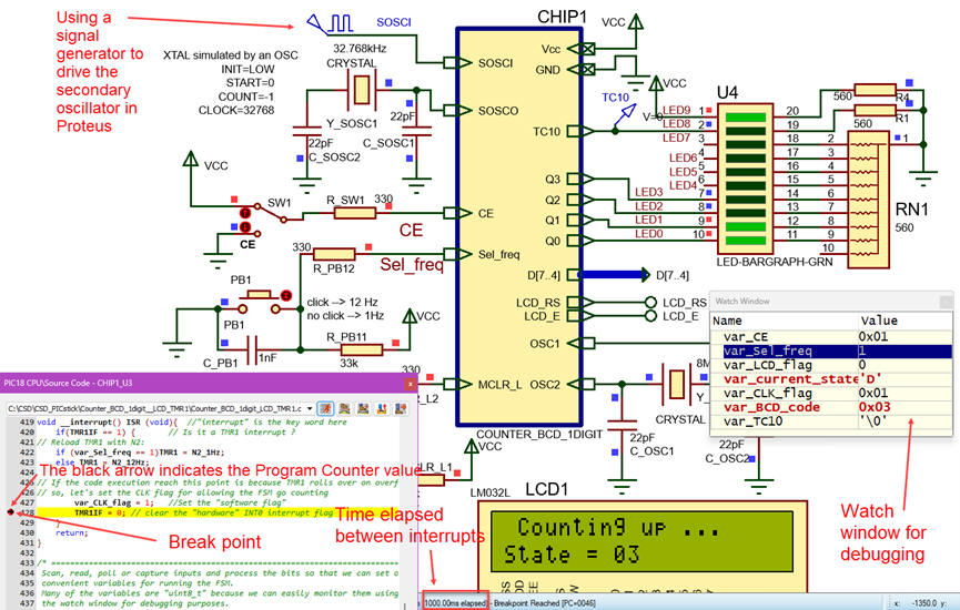
(4) Design phase #4: Counter_BCD_1digit_LCD_TMR1_AD. In order to check that the analogue input signal from the potentiometer AN0 is captured correctly, we can enhance the application adding analogue to digital (A/D) conversions. We can use the previous phase timing periods TP = 1 s or TP = 8.33 ms as sampling periods.
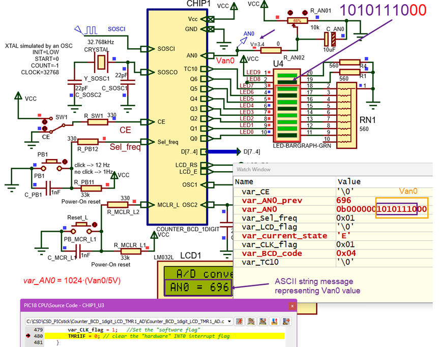 |
| Fig. 7. Counter_BCD_1digit_LCD_TMR1_AD captured in Proteus showing RAM variable is the watch window and all the mC pins in use. |
These final output files can be used to test whether the board is operating correctly once soldered: "Counter_BCD_1digit_LCD_TMR1_AD_prj.X.production.cof", ".elf", ".hex".
PCB design
We will capture the full circuit in a new KiCad project to draw the complete schematic and its PCB. Many additional components are required at this level: connectors, jumpers, footprints, power regulators, decoupling capacitors, etc.
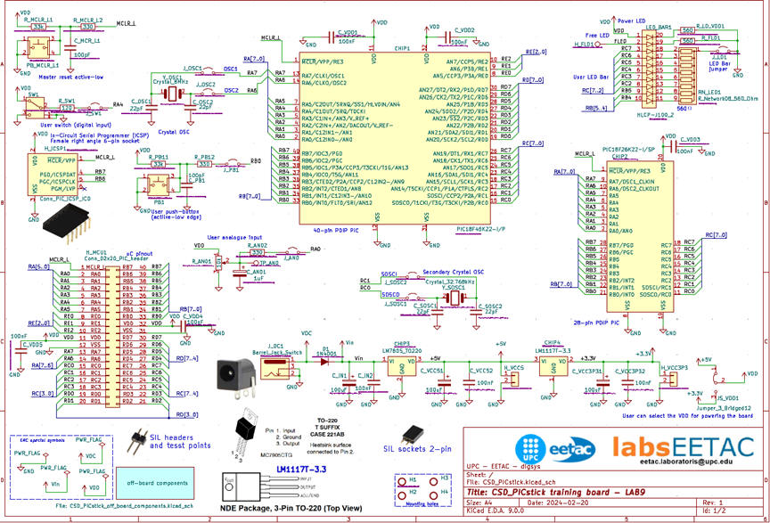 |
| Fig. 8. The PCB schematic contains many more resources, like headers, test points, etc. |
The full KiCad project "PCB_CSD_PICstick_v2.zip". Project location:
C:\CSD\CSD_PICstick\PCB\
 |
| Fig. 9. The 3D view of the finished board. |
NOTE: Our current CSD and DEE KiCad symbols, footprints, and 3D components are available in the library "DEE_libraries.zip" which can be unzipped and saved using these KiCad installation instructions. Basically, at this introductory PCB design level, the idea behind tuning component footprints is to enlarge their pads to make soldering easier.
You can use this prototype as a base model for copying and adapting your new application. Daughter or shield boards with additional components can be plugged through the 40-pin connector.
Another interesting option for developing a professional kit is miniaturise the prototype board selecting surface mount technology (SMT) components to be able to place components on both sides of the PCB.
Fig. 10 shows how the PCB can be manufactured in series at the same time that the bill of materials is generated from the EDA tool to order and buy all the required components.
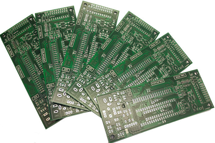 |
| Fig. 10. Several PCB ready for soldering components. |
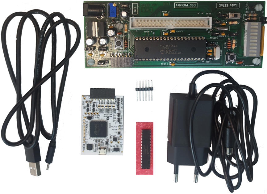
Fig. 11 is a picture showing all the materials included in the complete CSD_PICstick kit ready for mounting.
 |
| Fig. 11. CSD_PICstick components. |
Fig. 12 shows the typical prototyping testbench in the laboratory.
|
|
| Fig. 12. Laboratory bench including basic instruments and tools ready for soldering and testing the board. |
| Specifications | Planning | Developing | 4. Testing | Report |
PCB soldering step by step
Soldering components and testing is better done step by step checking that the few components attached works correctly running a simple application. The basic setup is shown in Fig. 13. The power adaptor and the MPLAB SNAP programmer will allow us to download application on the microcontroller.
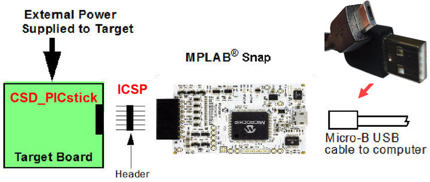 |
| Fig. 13. Target board, MPLAB SNAP and PC connection. |
Step #1. +5V regulator, chip socket, oscillator , reset push-button.
Connect a LED in a protoboard using two wires. Check that this LED blinking application works downloading the hex file by means of the MPLAB Programmer.
|
| Fig. 14. Mounting only step #1 components. |
Step #2 Solder the LED bar and the user PB1. Check that this LED blinking application works downloading the hex file by means of the MPLAB Programmer.
|
| Fig. 15. Mounting only step #1 components. |
Step #3 Solder the SW1, the secondary oscillator and the AN0 potentiometer. Check that this LED blinking application works downloading the hex file by means of the MPLAB Programmer.
|
| Fig. 16. Complete prototype. |
Testing the basic applications proposed in this tutorial
We can use the CSD_PICstick to test and debug the tutorial examples presented in this unit. The board is connected through the ICSP interface bus, as shown in Fig. 17, to the MPLAB SNAP in-circuit debugger and programmer.
Run any of the example phases in this unit to test whether the CSD_PICstick works correctly.
 |
| Fig. 17. Prototype ready for running an application. |
Using the CSD_PICstick with a protoboard adapter
We can connect other components through the 40-pin cable, starting with the protoboard adapter,
 |
| Fig. 18. Complete prototype ready for experimentation. |
We add here two experiments on programming the board with phase #4 application.
A) The first experiment connects the LCD peripheral on the protoboard using only the six wires.
 |
| Fig. 19. Phase #4 application running with a prototype connected using the six interface wires. |
B) The second experiment connects the LCD peripheral on the protoboard using the 40-pin flat cable as represented in Fig. 20 and an adapter.
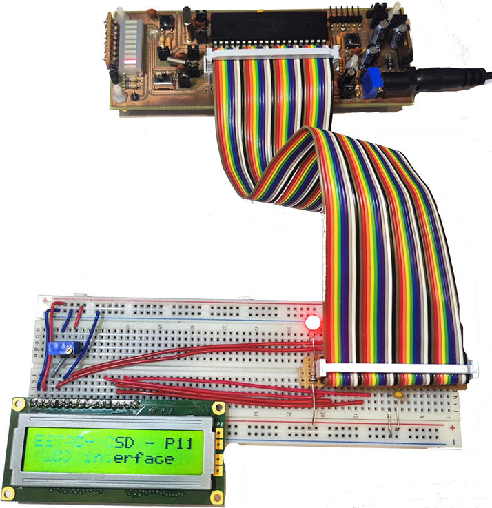 |
| Fig. 20. Phase #4 running with a prototype connected the 40-pin flat cable. |
You may continue the experiments measuring counter signals in a timing diagram using the VB8012 logic analyser as you did in Proteus. The expansion header represented in Fig. 21 may be used to monitor signals.
 |
| Fig. 21. 40-pin expansion header. |
The KiCad project of the protoboard adapter
Better to fabricate the 40-pin flat cable to protoboard adapter to connect the CSD_PICstick or any other similar board, to have full freedom for experimentation. The adapter represented in Fig 21. is required. These is the zipped KiCad file: "CSD_PCB_adapter_v1.zip".
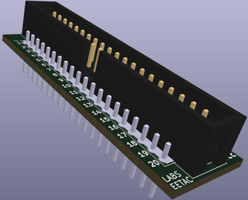 |
| Fig. 22. The KiCad 3D view of the 40-pin flat cable to protoboard adapter and the manufactured part. |
| Specifications | Planning | Developing | Testing | 5. Report |
Project report: sheets of paper, scanned and annotated figures, file listings, notes or any other resources. In CSD follow this rubric of indications for writing reports.
| Home Term 26/27-Q1 Contact Products Electronic devices and companies Software Books Magazines Instruments DEE Library EETAC DEEL |

|
|
| Web activa des de 09/2001, @ F. J. Robert, Web editat amb Microsoft Expression Web 4. El contingut és un complement als materials d'estudi del curs Circuits i Sistemes Digitals disponibles al campus digital Atenea. Llicència:Reconeixement 4.0 Internacional de Creative Commons |