|
|
Bachelor's Degree in Telecommunications Systems and in Network Engineering |
|
P7: standard sequential circuits: counters, data and shift registers |
| Resources in lectures and labs: | L7.1, Lab7, L7.2, L7.3 | Project | objectives |
Highlighted project: Counter modulo 24 with BCD outputs (Hour_counter)
| 1. Specifications | Planning | Developing | Test functional | Test gate-level | Report | Prototype |
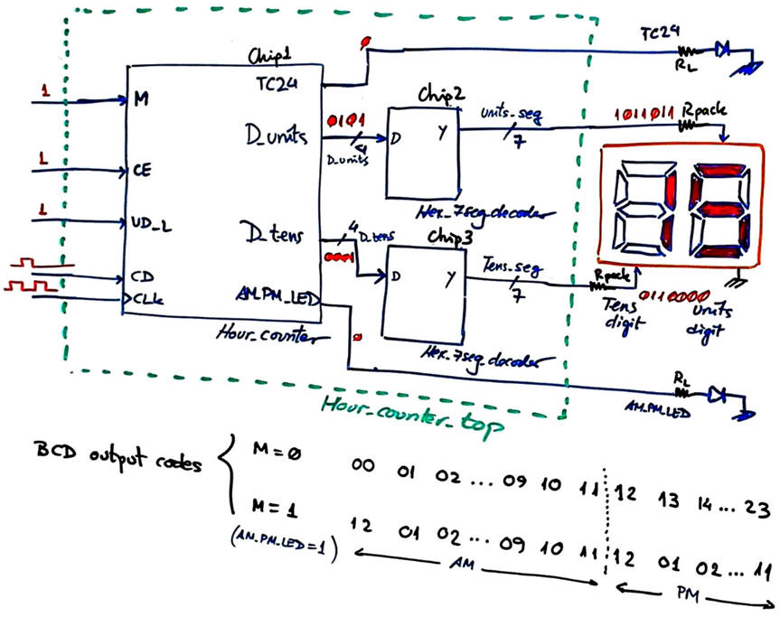
Our goal is to design an hour counter to be used in a real-time clock device to count hours in mode AM/PM when M = '1' and mode 00 ··· 23 when M = '0'. Fig. 1 represents the schematic diagram of the application when connected to 7-segment digits. Use plan C2 based on Counter_mod16 component and logic circuits.
 |
|
Fig 1. Symbol of the counter BCD modulo 24 (Hour_counter). The circuit Hour_counter_top shows how this block is used as a component in a larger project representing hours in 7-segment displays. |
Fig. 2 explain the function table of the Hour_counter discussing modes of operation.
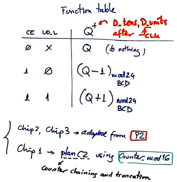 |
Fig 2. Function table determining the operating modes. When CE = '1' it counts up or down in modulo 24 using BCD codes. |
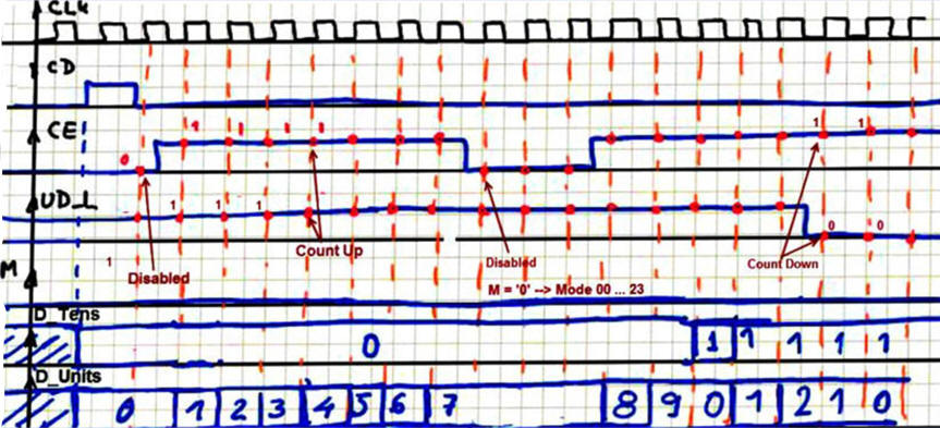
Fig. 3 is an example of timing diagram. How many states will the Hour_counter contain?
 |
|
Fig. 3. Example of timing diagram when M = '0' (representing hours from 00 to 23 format). |
Other design tutorials and assignments.
| Specifications | 2. Planning | Developing | Test functional | Test gate-level | Report | Prototype |
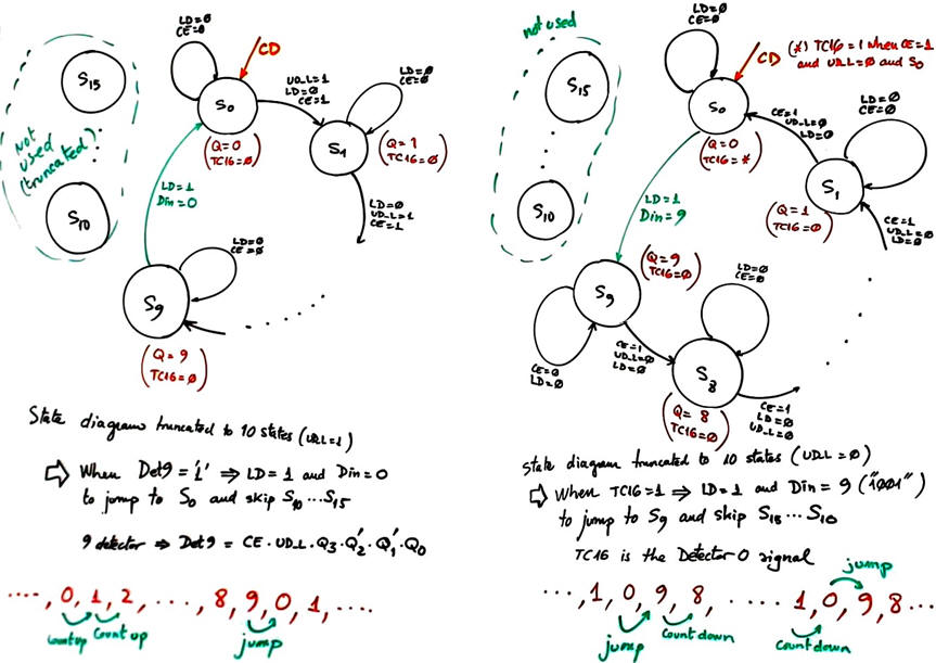
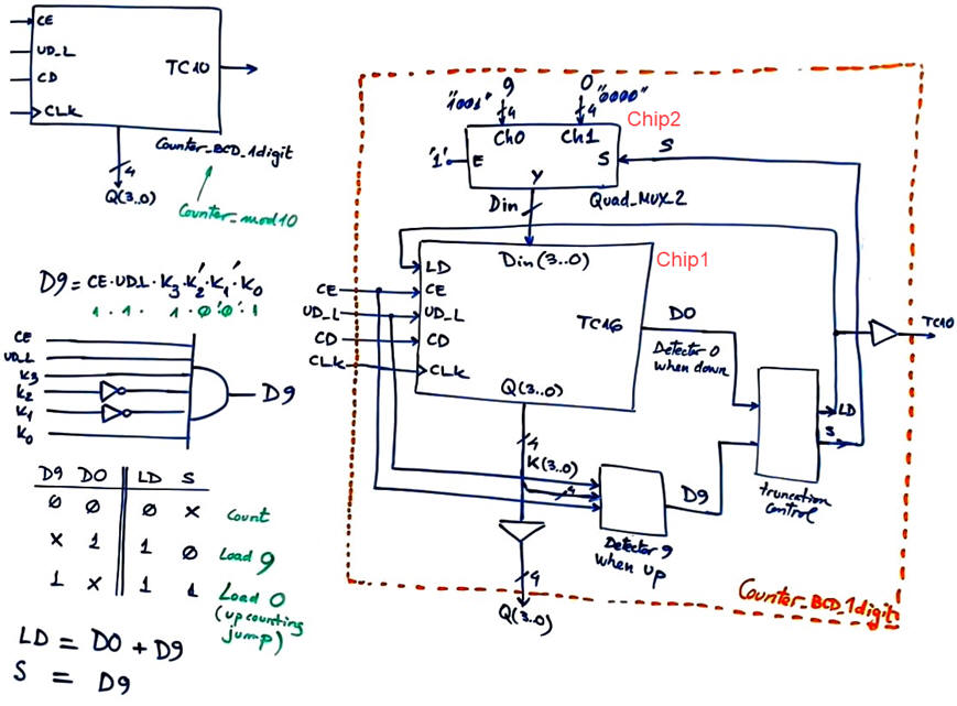
Design phase A: Counter_BCD_1digit using plan C2. To be able to count in BCD the first idea is truncating a larger counter like Counter_mod16 as shown in Fig. 4, thus inventing a Counter_BCD_1digit. A similar tutorial is discussed in Lab7 (Counter_mod12).
  |
|
Fig. 4. How to truncate a 4-bit binary counter to count in BCD. |
As you see, the idea is generating terminal count state detection signals for ordering parallel loading to jump to the desired state when counting up and also when counting down. Multiplexers are used to select the desired next state to go when jumping.
Design phase B: Hour_counter (or Counter_BCD_mod24)
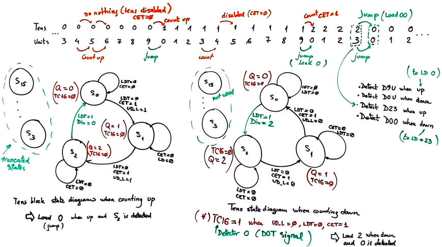
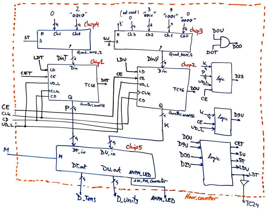
We can organise the internal architecture of the Hour_counter based on the use of universal 4-bit binary counters and combinational circuits and logic gates. For instance, considering BCD modulo 24 in Fig. 5, we infer when the circuit has to count and at which states it has to jump in order to truncate states not used. At the same time, we can think about chaining counters, we can determine when Tens digit is disabled and when it can advance (CET, counter enable tens control signal).
  |
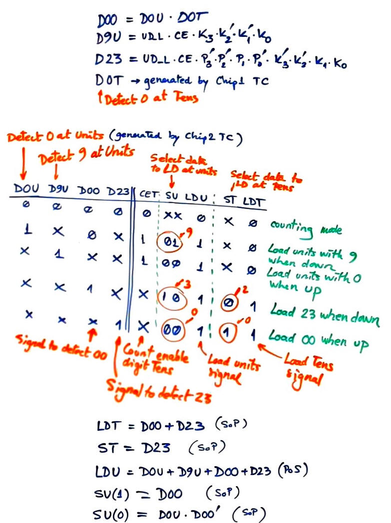 a) Counter BCD modulo 24 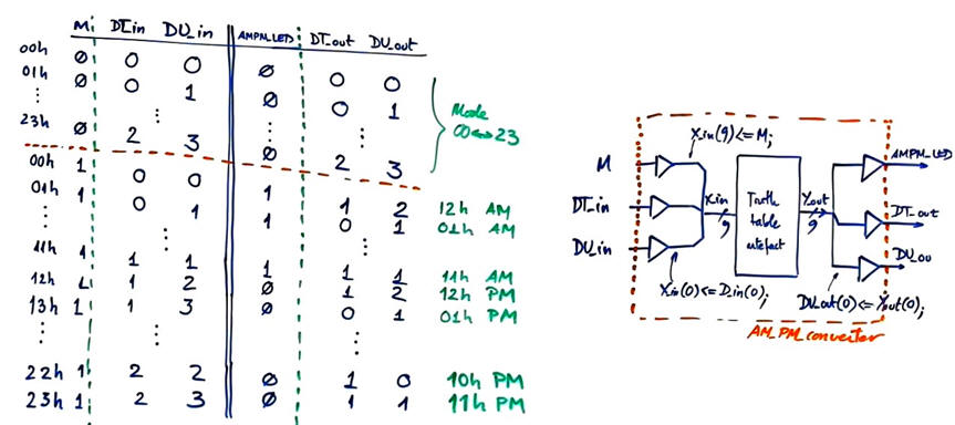 b) Truth table for converting results to mode AM-PM. Plan B interpretation using the truth table artefact. |
|
Fig. 5. Plan C2 for organising the Hour_counter using truncation and chaining techniques. |
Project location:
C:\CSD\P7\Hour_counter\(files)
How many VHDL files will be required to complete the Hour_counter?
How many D_FF this project will contain?
| Specifications | Planning | 3. Developing | Test functional | Test gate-level | Report | Prototype |
Translate the hierarchical top schematic in Fig. 5 to VHDL as Hour_counter.vhd. Use the Counter_mod16 as component and also these Quad_MUX_2.vhd and Quad_MUX_4.vhd from P2. This is the AM_PM_converter.vhd.
Start an EDA synthesis project for a given target PLD (any CPLD or FPGA available in the laboratory). Inspect the project summary. Inspect the RTL and technology views. Comment them and check the number of DFF used.
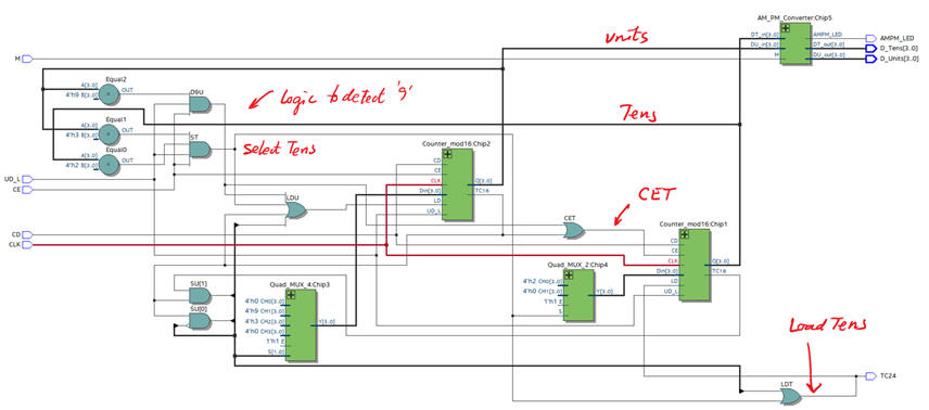 |
Fig. 6. RTL view. |
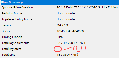 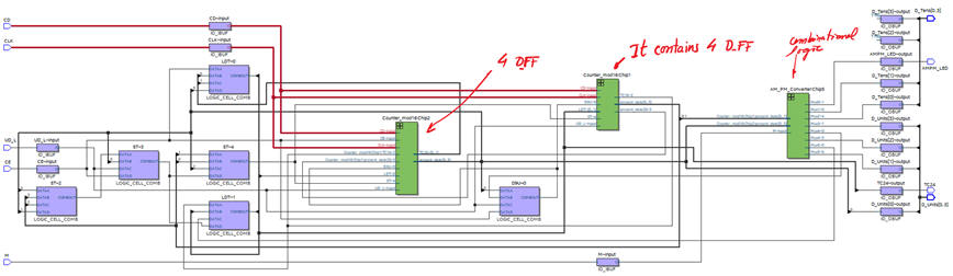 |
Fig. 7. Technology view. |
| Specifications | Planning | Developing | 4. Test functional | Test gate-level | Report | Prototype |
Start the test bench template and add the CLK and inputs activity translating the timing diagram in Fig. 3. Make all time values relative to the CLK_Period constant.
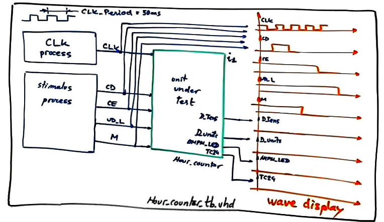 |
Fig. 8. Testbench schematic fixture. Hour_counter is a subsystem that usually will be connected after a MM:SS counter module in real-time clock systems, thus the real CLK period will be one hour. In order to test the circuit we choose CLK_Period = 50 ms, to speed up simulations ( > run 4000 ms). |
Generate from Quartus Prime the testbench fixture skeleton in Fig. 8. Rename it and move it to the project folder.
Copy from this example file Hour_counter_tb.vhd only the stimulus activity described in the two processes and also the constant CLK_Period.
Start and run a functional simulation project using ModelSim to verify that the device operates like expected in the initial timing diagram sketch in Fig. 3.
Fig. 9 shows how a functional simulation of the Hour_counter module can be performed. In this case representing the waveforms for M = '1' when the circuit works in AM-PM mode.
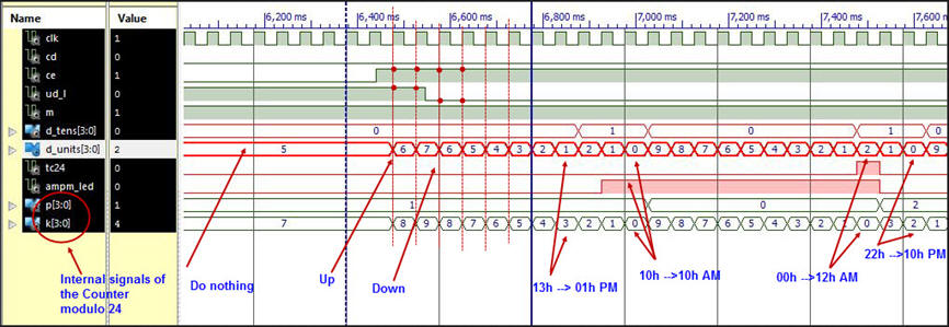 |
| Fig 9. Hour_counter waveforms in functional simulation for M = '1'. |
| Specifications | Planning | Developing | Test functional | 5. Test gate-level | Report | Prototype |
Run a gate-level timing simulation to measure the maximum speed of the counter deduced from the propagation time from CLK to output (tCO). We have to choose a MAXII or a Cyclone IV FPGA. MAX10 technology do not generate SDO files for running gate-level simulations.
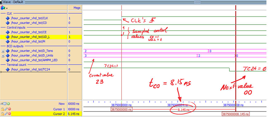 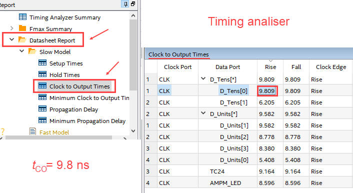 |
| Fig 10. Measuring tCO for a target chip MAXII. It means that the maximum CLK frequency is fMAX = 1/ tCO = 102 MHz. |
| Specifications | Planning | Developing | Test functional | Test gate-level | 6. Report | Prototype |
Follow this rubric for writing reports.
| Specifications | Planning | Developing | Test functional | Test gate-level | Report | 7. Prototype |
Choose a laboratory experimentation board like DE10-Lite from Terasic. Build the prototype Hour_counter_top in Fig. 1 adding the necessary chips and modifications to adapt it to the board's hardware. Assign FPGA pins. As we did with simulations, to speed up counts we can use a CLK_2Hz_SQ signal from a CLK_generator component.
Optional. This Hour_counter circuit allows you to imagine how the project of a complete HH:MM:SS real-time clock circuit may be designed. It can even be enhanced including a YY:MM:DD calendar. How to adjust the number of days for each month? How to include February leap years where the day 29th is included?
| Home Term 26/27-Q1 Contact Products Electronic devices and companies Software Books Magazines Instruments DEE Library EETAC DEEL |

|
|
| Web activa des de 09/2001, @ F. J. Robert, Web editat amb Microsoft Expression Web 4. El contingut és un complement als materials d'estudi del curs Circuits i Sistemes Digitals disponibles al campus digital Atenea. Llicència:Reconeixement 4.0 Internacional de Creative Commons |