|
|
Bachelor's Degree in Telecommunications Systems and in Network Engineering |
|
|
|
|||
|
|
1-digit BCD counter with LCD and TMR0 (LAB10 design phase #3)TMR0 as counter of external events TMR0 as timer |
|
|
|
|
|||
To learn how to apply the TMR0 peripheral we can imagine two options for completing the LAB10 design phase #3:
- Option TMR0 as counter of external events
Replace the external CLK connected at INT0 (RB0) by the internal TMR0 to generate the same var_CLK_flag using the pin T0CKI (RA4). In this way TMR0 is a counter device to trigger TMR0IF after counting a number N of external CLK period.
- Option TMR0 as timer
We can imagine replacing the external CLK oscillator by the internal TMR0 used as a timer triggering interrupts for setting var_CLK_flag after a given timing period TP. The idea is to count pulses from the quartz OSC internal reference time base TB = 4·TOSC. The timing period TP can be set to any duration using N3 as a post-scaler software variable: TP = TB·N1·N2·N3. As an alternative, TMR2 can be used in the same way.
| 1. Specifications | Planning | Dev. & test | Prototype | report |
(updating to the PIC18F46K22 in progress)
FSM + plan X + Interrupts + LCD + TMR0 (as a counter of external events)
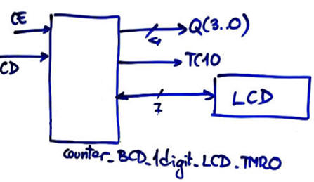
In this tutorial we propose to solve A). TMR0 peripheral configured as counter. The idea is to free the INT0 (RB0) pin used in the two previous design phases so that it can be used in any other future application while being able to continue counting external events. Imagine the Counter_BCD_1digit_LCD_TMR0 counting every N = 3 external CLK pulses.
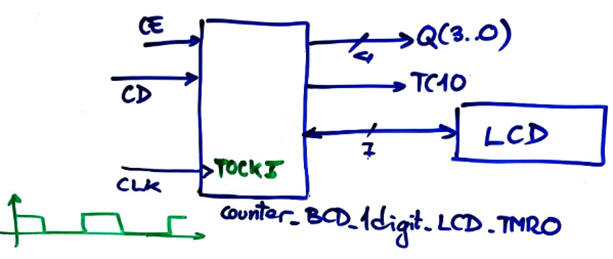 |
Fig 1. Symbol of the device to be designed. TMR0 CLK input (T0CKI) is connected to RA4 pin. |
| Specifications | 2. Planning | Dev. & test | Prototype | report |
Most of the planning is inherited from design phase #2 and there is no need to report it again. Let us focus simply on what changes when TMR0 is used as counter attached to RA4/T0CKI pin to replace the external interrupt RB0/INT0.
A) Planning hardware
INT0 (RB0) is left unconnected and RA4 (T0CKI) is used as the CLK input for the hardware counter peripheral TMR0. Fig. 2 shows its internal design. The prescaler can also be used to set the number of N pulses to count before triggering a TMR0IF interrupt.
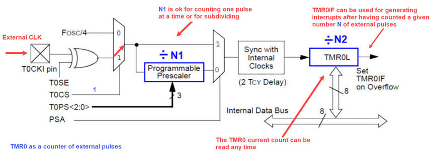 |
Fig. 2. When using TMR0 as counter we have two possibilities: a) We can read (poll) the current TMR0 register value, or b) we can wait for interrupt TMR0IF on overflow. |
The simplified schematic in Fig. 3 shows the block diagram adjusted to this application where the number of pulses counted before TMR0IF are N = N1·N2. The parameter N1 is the prescaler value. The parameter N2 = (256 - NP) in 8-bit mode or NP = (65536 - NP) in 16-bit mode.
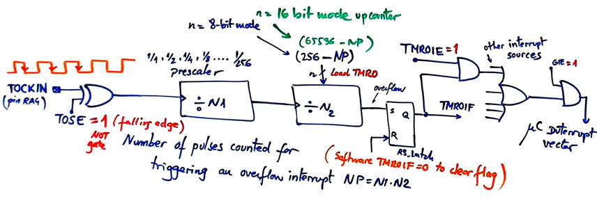 |
Fig 3. TMR0 as counter of N = N1·N2 pulses before triggering interrupt TMR0IF. |
B) Planning software
The hardware-software diagram has to reflect that the var_CLK_flag variable is obtained using the TMR0 peripheral.
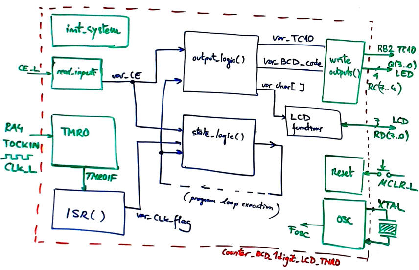 |
Fig. 4. Hardware-software diagram. |
init_system() includes the TMR0 initialisation as counter. We have to program the configuration bits in T0CON control register accordingly.
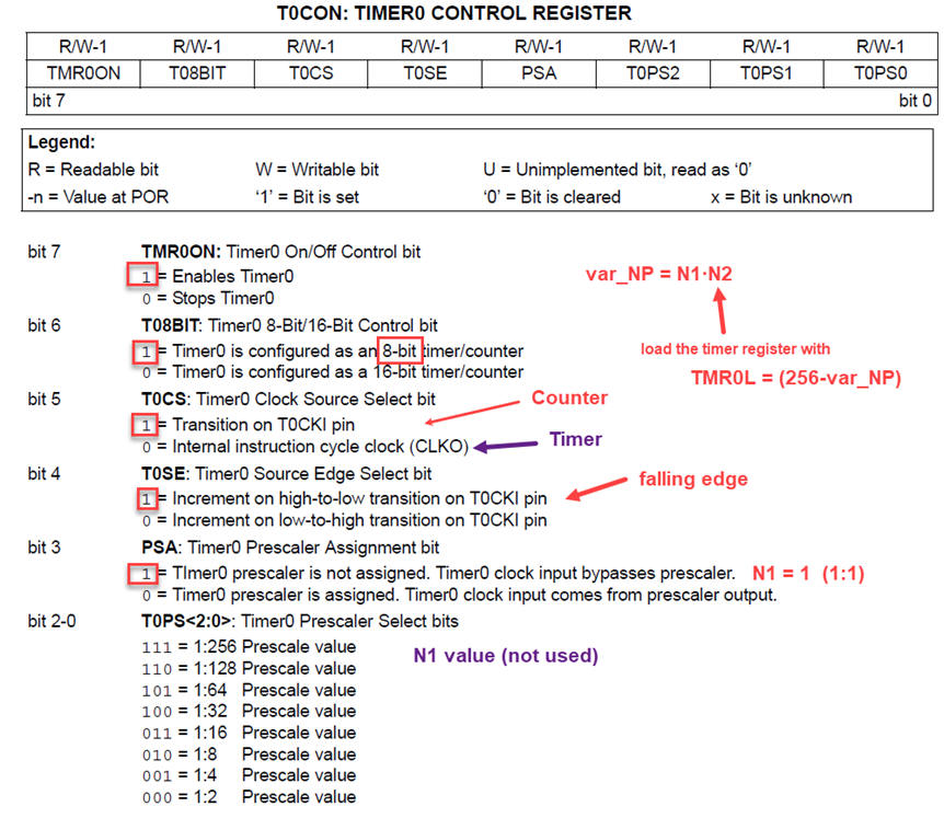 |
Fig. 5. TMR0 setup as a counter in init_system(). |
ISR() is intended to generate var_CLK_flag when TMR0IF is detected (as it was in previous design phases for INT0IF). TMR0IF will be triggered after N = N1· N2 external CLK period.
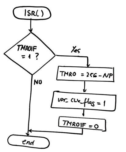 |
Fig. 6. ISR() flowchart to attend TMR0 interrupts. We have to reload the counter initial value N2 every interrupt event so that only NP pulses are counted before triggering another interrupt. Note how the hardware flag TMR0IF is reset before returning from interrupt to the main program loop. |
Organise an MPLABX - XC8 IDE project targeting a PIC18F4520 at location:
C:\CSD\P12\counter_BCD_1digit_LCD_TMR0\(files)
| Specifications | Planning | 3. Dev. & 4. test | Prototype | report |
A) Developing hardware
NOTE: In order to avoid warnings and complications regarding project names and folder path length, we will shorten them.

New project location:
C:\CSD\P12\c_BCD_1d_LCD_TMR0\(files)
Example circuit capture: c_BCD_1d_LCD_TMR0.pdsprj.
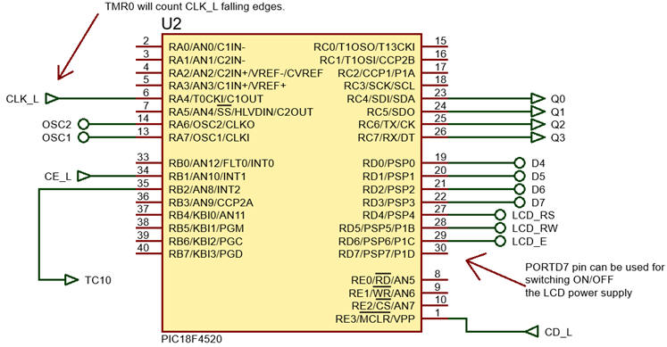 |
Fig. 7. Connect CLK_L terminal to RA4 pin. |
B) Developing software
This is the proposed source code c_BCD_1d_LCD_TMR0.c to be compiled along with the LCD library functions in the new project c_BCD_1d_LCD_TMR0_prj. Compile the project to generate executable files.
C) Step-by-step testing
Run the Proteus simulator. Do it in step by step mode while watching variables and placing break points, specially for following interrupt flags.
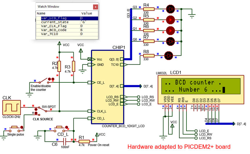 |
| Fig. 8. The circuit in "run" mode while monitoring the variables in the "watch" window. This top schematic is the same as in design phase #2; users see no differences between design phases #2 and #3. |
Pay attention on visualising var_CLK_flag.
Check that the design step #2 works as expected: BCD count will advance every NP = 3 pulses (or any other value).
| Specifications | Planning | Dev. & Test | 5. Prototype | Report |
| Specifications | Planning | Dev. & Test | Prototype | 6. Report |
Follow this rubric for writing reports.
|
|
1-digit BCD counter with LCD and TMR0 (LAB10 design phase #3)TMR0 as counter of external events TMR0 as timer |
|
| 1. Specifications | Planning | Dev. & test | Prototype | TMR0_timer_report |
FSM + plan X + Interrupts + LCD + TMR0 (as a timer)
In this second tutorial we propose to configure TMR0 peripheral as timer. The idea is to keep timing a given period TP without using external interrupts, liberating such pins for other applications. We can use the internal time base TB = 4/FOSC as a time reference. Let us generate a fixed timing period of TP = 500 ms (2Hz) for counting in BCD.
 |
| Fig 1. Symbol of the device to be designed. TMR0 is used to obtain a timing period TP = TB·N1·N2·N3 to set var_CLK_flag counting pulses derived from the internal XTAL oscillator. |
Optional. To discover how to use other peripherals in this application, we can imagine another design phase #5: BCD counting using an adjustable var_CLK_flag period TP by means of a potentiometer connected to an A/D input (1024 values, 10-bit converter. For example from TP = 1 ms to TP = 1 s.
| Specifications | 2. Planning | Dev. & test | Prototype | TMR0_timer_report |
| Specifications | Planning | 3. Dev. & 4. test | Prototype | TMR0_timer_report |
| Specifications | Planning | Dev. & Test | 5. Prototype | TMR0_timer_report |
| Specifications | Planning | Dev. & Test | Prototype | 6. Report |
Follow this rubric for writing reports.
| Home Term 26/27-Q1 Contact Products Electronic devices and companies Software Books Magazines Instruments DEE Library EETAC DEEL |

|
|
| Web activa des de 09/2001, @ F. J. Robert, Web editat amb Microsoft Expression Web 4. El contingut és un complement als materials d'estudi del curs Circuits i Sistemes Digitals disponibles al campus digital Atenea. Llicència:Reconeixement 4.0 Internacional de Creative Commons |