|
|
Bachelor's Degree in Telecommunications Systems and in Network Engineering |
|
P9: introducing microcontrollers (μC). Digital I/O and programming |
| Resources in lectures and labs: | L9.1, Lab9, L9.2, L9.3, L9.4 | Project | objectives |
Highlighted project: 1-digit BCD adder (design phase #1)
| 1. Specifications | Planning | Dev. & test | Prototype | report |
The aim of this project is to solve a combinational circuit 1-digit BCD adder (Adder_BCD_1digit) type MC14560 using a microcontroller (μC) to learn the basics of these devices. This chip is not new for you because it could have been proposed in P3 as another arithmetic circuit, thus we may focus our efforts in the new μC technology to implement it.
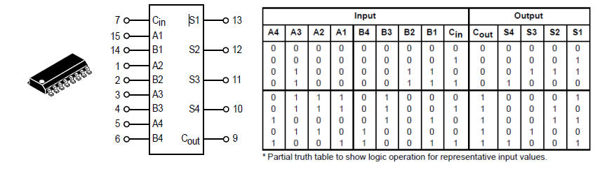 |
| Fig 1. Classic chip MC14560 that we try to recreate as a way to learn on digital inputs and outputs and code organisation in a microcontroller. |
This goal implies:
1) Getting in touch with a commercial μC from Microchip, for instance the PIC18F46K22, learning how to compile C language code using MPLABX + XC8 tools and simulate the project using Proteus. And also:
2) Study how C code is organised in CSD to translate our diagrams, configure digital inputs and outputs and connect program variables to pins using bitwise operations (OR, AND, etc.)
 |
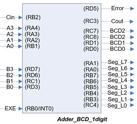
| Fig 2. Symbol of the 1-digit BCD adder indicating the port pins where to connect input and outputs. |
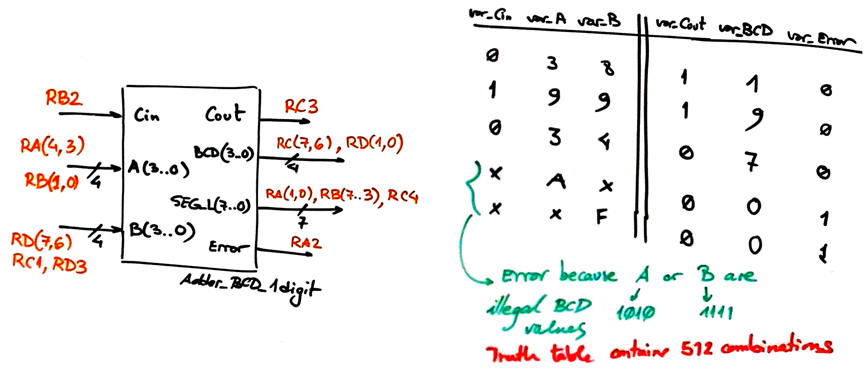
Add other example values to the truth table of this device. Why we need to implement as well an error signal in this application?
See how we conceive the truth table using RAM variables instead of signals: var_A instead of A, var_Cin instead of Cin.
Other design tutorials and assignments.
| Specifications | 2. Planning | Dev. & test | Prototype | report |
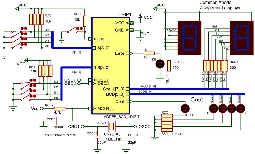
A) Planning hardware
Draw your circuit in a sheet of paper and discuss where to connect: reset (MCLR_L), crystal oscillator (OSC1, OSC2)and digital I/O. Add as well the 7-segment displays to shown the BCD result.
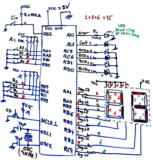 |
| Fig 4. Hardware schematic. |
B) Planning software
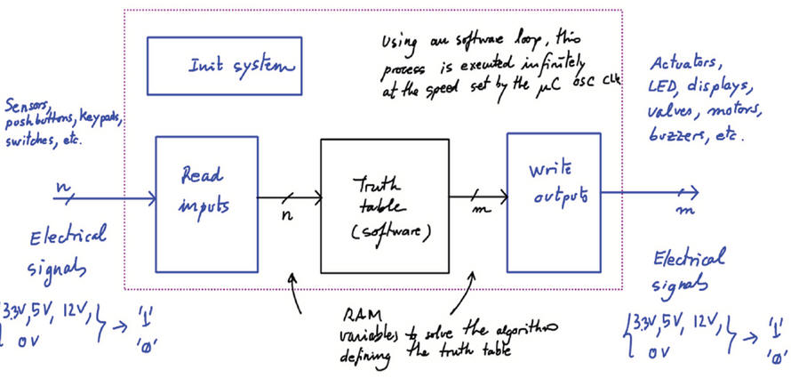
Our CSD style is reflected in the new conceptual tool for representing how to put into practice our design ideas: the hardware-software diagram as represented in Fig. 5. The key point is to define RAM variables (char, int, double int, etc.) that will allow the processing of the algorithms without regarding the way PORT pins have been read or written. Thus, the kernel of the code (in this case truth_table() function) is hardware independent or is abstracted from hardware dependencies.
Pay attention that hardware-dependent functions (input, output and system initialisation) and software (or platform independent) functions (the truth table) are drawn using different colours to emphasise this point.
 a) 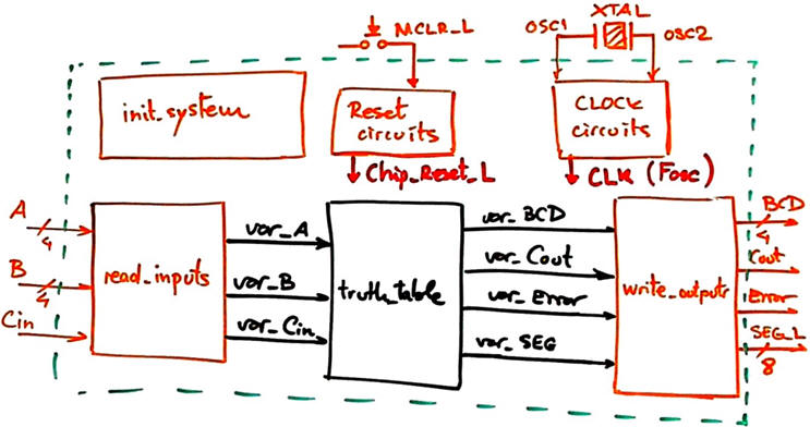 b) |
Fig 5. The new conceptual representation tool: a) hardware-software diagram ideas, b) the application to this project. |
Organise the source code as in Fig. 6 using program flowcharts: Init_system(), read_inputs(), truth_table() (which is the algorithm or data processing) and write_outputs().
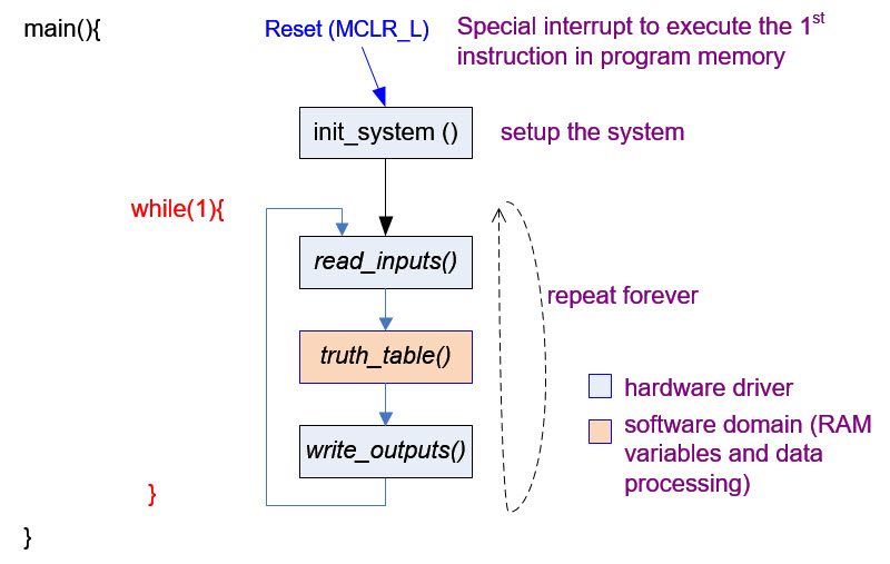 |
| Fig. 6. Proposed software organisation flowchart in CSD. |
RAM variables (var_SEG_L is not yet represented, and this is not a problem, because you can add new features to your basic project later, once it works; this is the important idea of planning several design steps and phases).
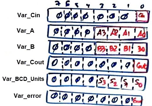 |
Fig. 7. Example of some convenient variables "var" that will allow the processing of information in truth_table() independently of the microcontroller hardware. Program variables will be stored in RAM memory addresses and so, they are volatile. |
When we initialise the system, we configure microcontroller bi-directional port pins to be unidirectional: only inputs or only outputs. Here, we will consider all unused port pins outputs as default. We do this configuration using the TRI-State control register (TRISx) bits. Saving a zero ('0') means output. Saving a one ('1') means that the pin will be an input. More information on pin configurations and tri-state technology.
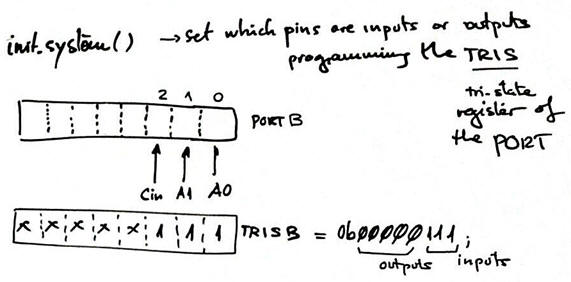 |
| Fig. 8. init_system() function details. Shadow register TRISx values, bits of interest. |
Read inputs. How to capture and transfer input voltages into RAM variables
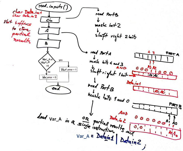 |
| Fig. 9. read_inputs() function: flowchart, operations, memory diagram, bits of interest, etc. |
Write outputs. How transfer RAM variables into port pin digital voltages.
 |
Fig. 10. write_outputs() flowchart. |
Behavioural plan B for translating a truth table into a flowchart and C language.
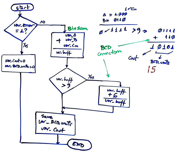 |
Fig. 11. truth_table() function flowchart. As usual, use basically rhombus or diamond shapes for decisions or yes/no questions and rectangles for actions or operations. |
Plan a sequence for building and debugging the application: the idea is "plan & develop & test" step by step introducing a few lines of code at a time. For instance:
1) Solve the code for reading only the Cin pin, compile, run and test the var_Cin variable using the watch window.
2) Add the code for reading only the operant A, run, test and watch var_A, etc.
NOTE: You may also consider several design steps. For instance:
Step #1. Solve the circuit using only switches, buttons and LED as represented in Fig. 5. And only when the system is working correctly, consider the next step:
Step #2. Add the extra RAM variables and modify the hardware and software to interface the 7-segment display.
Project locations and file names:
C:\CSD\P9\Adder_BCD_1digit\(files)
| Specifications | Planning | 3. Dev. & 4. test | Prototype | report |
A) Developing hardware
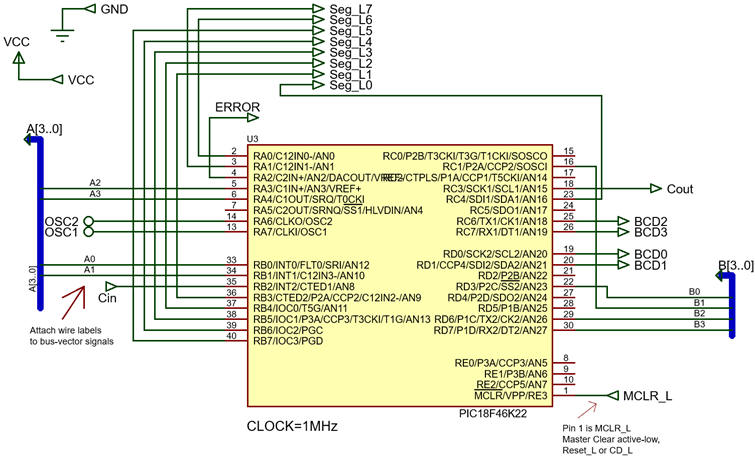
Draw the schematic of the application in Proteus copying an example or tutorial which already contains the microcontroller that you have to use. Target μC PIC18F46K22: "Adder_BCD_1digit.pdsprj".
   |
|
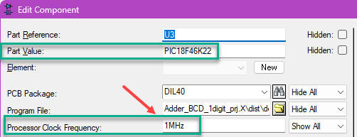
Fig. 12. The Adder_BCD_1digit symbol and electrical connections as captured in Proteus. You can also see the internal architecture (child sheet) based on the PIC18F46K22. Be aware that in Proteus the clock frequency for simulation is set using the Processor Clock Frequency parameter. It can be as high as 64 MHz. |
Similar legacy schematics targeting other μC: PIC18F4520: "Adder_BCD_1digit.pdsprj"; Atmega8535: "Adder_BCD_1digit.pdsprj".
B) Developing software
Install MPLABX + XC8 software development environment
Run the microcontroller's IDE to develop and compile the C code copying and adapting an example code. Example C file targeting the PIC18F46K22: "Adder_BCD_1digit.c". Add to your project the header file "config.h".
 |
|
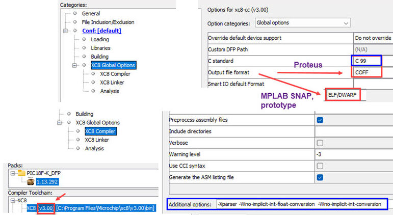
Fig. 13. Selecting the compiler options: C standard C99. Output file COFF for running Proteus. To disable some warnings you can add these additional XC8 Compiler options: -Xparser -Wno-implicit-int-conversion -Wno-implicit-int-float-conversion. |
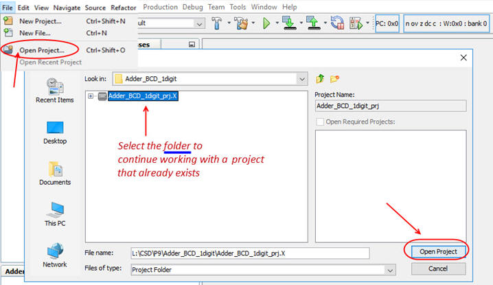
NOTE: If your project was created in a previous session and you like to continue working on it, simply click Open Project and select the project folder.
 ç ç |
|
Fig. 14. Opening a project already created clicking on the folder. |
Similar legacy code targeting other legacy μC: PIC18F4520 --> "Adder_BCD_1digit.c"; PIC16F877A --> "Adder_BCD_1digit.c".
C) Step-by-step testing
Develop, compile and debug step by step interactively according to your plan, testing if it works before adding new code. For example, as indicated in the planning above, complete the operations for watching the var_Cin variable; then repeat it all for watching the variable var_A, and so on. Use tutorial examples to copy and adapt the C source file. Remember that, as usual, C code is not valid unless you are translating a flowchart, which is equivalent to translating some algorithm or truth table.
Run the Proteus simulator. Do it in step by step mode while watching variables and placing break points.
Important Note: The memory addresses for variables can change after recompilation, specially when rewriting and adding new code. If you recompile your project, you may need to delete and re-add the variables in the watch window to ensure the correct values are displayed.
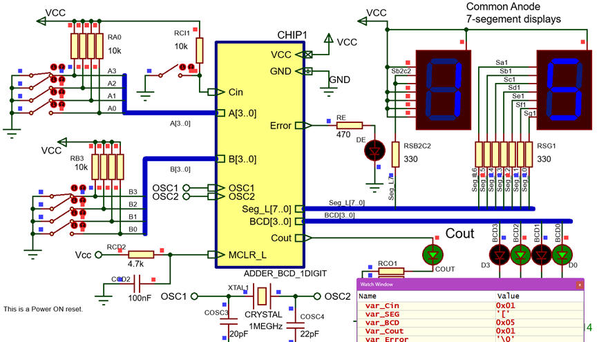 |
| Fig. 15. The circuit in "run" mode while monitoring RAM variables in the "watch" window. |
Some ideas for discussion:
- Does the program simulation work the same for several crystal oscillator frequencies: 1 MHz, 2 MHz, 8 MHz, etc.?
- How long does it take to run the main loop? How many times per second is executed the main loop, or equivalently, at which frequency are sampled or read the input signals?
- How does it compare to the same circuit solved in Chapter I using VHDL in an FPGA target chip?
| Specifications | Planning | Dev. & Test | 5. Prototype | Report |
Example 1: Board CSD_PICstick, target microcontroller: PIC18F46K22, tools: MPLAB X + XC8 + Proteus + MPLAB SNAP in-circuit debugger-programmer.
Prototyping, for this initial project means basically testing the installation of developing tools and using the CSD_PICstick 40-pin connector to attach switches and LED.
|
|
Fig. 16. CSD_PICstick board, protoboard and programmer for running the experiment. |
| Specifications | Planning | Dev. & Test | Prototype | 6. Report |
Check that you can answer most of this basic questions on mC after having solved this introductory project. Follow this rubric for writing reports.
Annex
Optional project: that can be imagined as the next design phase #2: Add the EXE key (interrupts, edge detection)
A good example to see how the interrupt mechanism for detecting signal edges works is for instance: modify the design in this tutorial so that the truth table is calculated only when EXE pushbutton is pressed. This means that even if we modify the input operands, the new result will be displayed only after clicking EXE.
 |
|
Fig. 1. Adder_BCD_1digit circuit modified with EXE input. |
Some ideas to organise the project:
- Copy Adder_BCD_1digit.pdsprj to the new project folder and adapt the hardware circuit from P9. Project locations and file names:
C:\CSD\P9\Adder_BCD_1digit_EXE\(files)
- Study the INT0 mechanism and how it is configured in init_system(). Consider the hardware flag INT0F and its software variable: var_EXE_flag.
- Modify the software flowchart so that truth_table() is executed only once var_EXE_flag is set.
- Write the software source file Adder_BCD_1digit.c. Start an MPLABX - XC8 project targeted to the PIC18F46K22 chip.
- Start compiling and testing (debugging) interactively watching variables and using step-by-step execution.
- How long does it take to execute the ISR()?
| Home Term 26/27-Q1 Contact Products Electronic devices and companies Software Books Magazines Instruments DEE Library EETAC DEEL |

|
|
| Web activa des de 09/2001, @ F. J. Robert, Web editat amb Microsoft Expression Web 4. El contingut és un complement als materials d'estudi del curs Circuits i Sistemes Digitals disponibles al campus digital Atenea. Llicència:Reconeixement 4.0 Internacional de Creative Commons |