|
|
Bachelor's Degree in Telecommunications Systems and in Network Engineering |
|
|
|
||
|
|
Synchronous 1-digit BCD counter |
|
|
|
||
Plan X: FSM with state signals as state enumeration (as all P6 projects)
1. Specifications
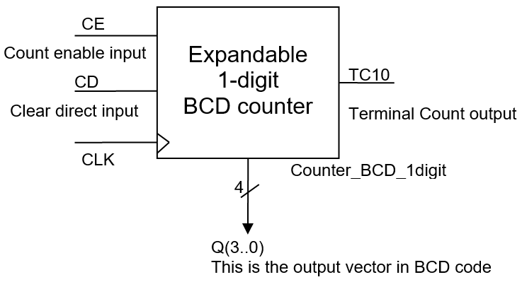
Design a synchronous 1-digit BCD counter following a FSM strategy where all the states will be enumerated. The chip will include an asynchronous reset (CD) and also a count enable (CE) input and a terminal count (TC10) output to allow expandability. rec.
|
|
|
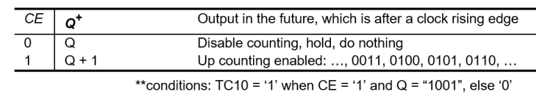
| Fig. 1. Symbol and function table. You can also draw an example timing diagram for this circuit. | |
It is a good idea to read a typical datasheet of a classic chip that has similar features, like the 74LS162. And it is also necesary to draw an example sketch of timing diagram to be able to apply the function table.
|
|
|
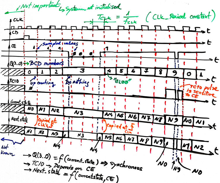
| Fig. 2. An example timing diagram for this counter. Solve it in a sheet of paper annotating on the waveforms all the important details over time. You can also represent the evolution of the internal FSM signals current_state and next_state. The VHDL testbench functional simulation in the 4th design step is based on the translation of a diagram like this one. | |
The circuit in Fig. 3 is the complete example project solved using the Lattice ispLEVER Classic and Proteus ISIS so that the counter can be downloaded into a simple sPLD GAL22V10 target chip. In order to run it, download and unzip the compressed file in a given folder. The GAL symbol is connected to the binary configuration file counter_BCD_1digit_prj.jed where the sPLD fuses are programmed.
|
|
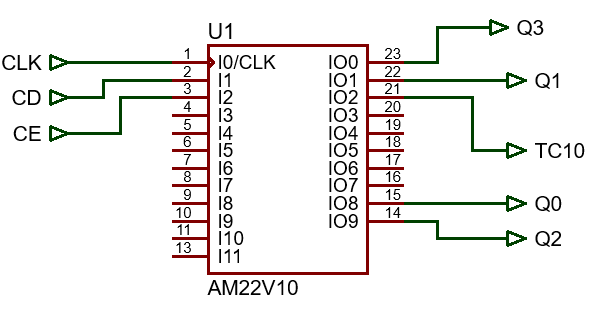
| Fig. 3. Schematic and pinning for the counter when targeting a sPLD GAL22V10. |
This is an example where such circuit can be used as a component (plan C2) to invent larger counters of the same kind: the design on a 2-digit BCD counter (Counter_BCD_mod100) chaining two 1-digit BCD counter blocks in Proteus.
2. Planning
Let's apply the FSM methodology to build the counter. Thus, as you have seen in the tutorials, we'll follow always the same methodology to improve understanding and the reliability of the circuits designed. rec.
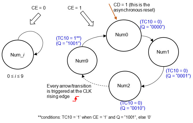
1) Figure out the state diagram. Number of states and conditions of transitions. Outputs at each state. In this example, there are 10 states and 20 state transitions.
 |
|
|
Fig. 4. State diagram where the arrows indicate the transitions between states accordingly to the given condition, and in parenthesis in each state the is the indication of the output values. To make it easy, different colours are used to represent outputs and transitions. |
|
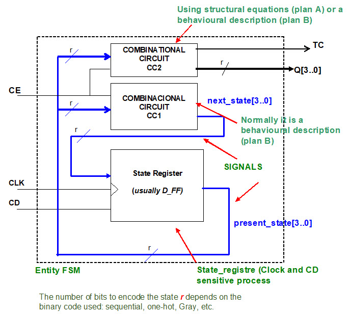
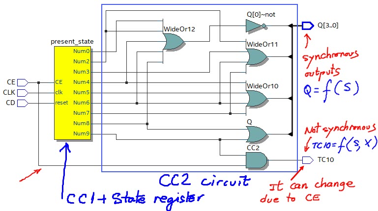
2) Customise the general FSM topology to this problem indicating where all the inputs and outputs are connected. The number of bits r for coding in binary the current and next states will depend on the binary code used and the number of states. [r = number of states if one-hot code; r = (1/log 2)·log (number of states) if binary or Gray code].
 |
|
|
Fig. 5. The general topology of a finite state machine (FSM) particularised for this problem supposing that the current state is coded in binary-sequential (r = 4 bits). |
|
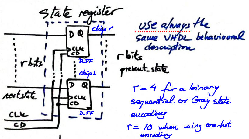
3) State register. We'll use always the same VHDL code description, which corresponds to the process of an r-bit D_FF with asynchronous reset. Draw the state register schematic.
 |
|
|
Fig. 6. Sketch of the state register memory circuit, r D_FF working synchronously in parellel. |
|
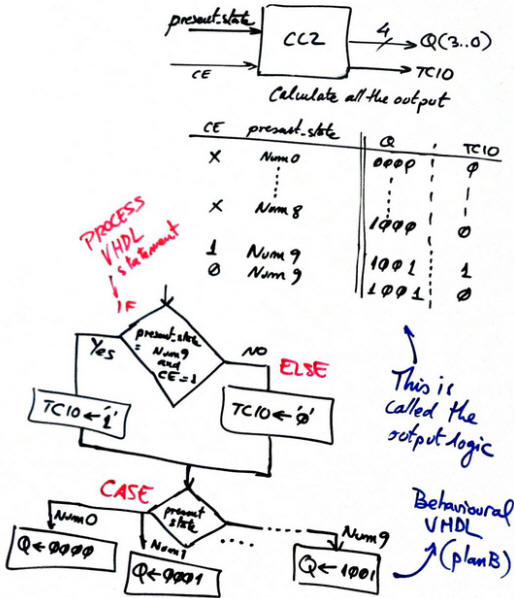
4) CC2 in Fig.7. Truth table and its behavioural description as a flowchart (plan B). The synthesiser will generate the final circuit from this process. The CC2 is required to calculate the outputs at each state. The outputs in the state diagram are annotated in parenthesis and in a different colour. Note how it is possible to solve different output sequences of binary codes simply redesigning the CC2 truth table. CC2 is acting as a code converter.
 |
|
|
Fig. 7. The truth table of the blocks CC2 and its equivalent flochart. CC2 generates all the outputs represented in parenthesis in each state. |
|
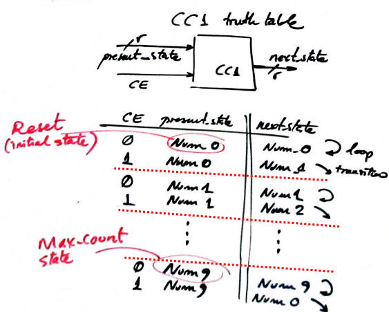
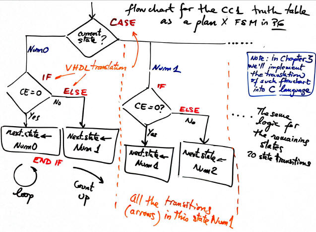
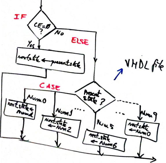
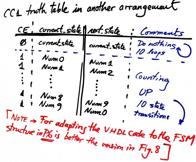
5) CC1 in Fig.8. Truth table and its behavioural description as a flowchart (plan B). The synthesiser will generate the final circuit from this process. CC1 is required to calculate the next state to go after the CLK's rising edge.
Note: there is another behavioural interpretation in case of representing the CC1 truth table reordered differently than in Fig. 8.
  |
|
|
Fig. 8. The truth table of the blocks CC1 and its equivalent flochart for executing all the state transitions represented as arrows in the state diagram. |
|
6) The project name Counter_BCD_1digit_prj and folder location to develop the product:
L:/CSD/P7/Counter_BCD_1digit_X/(files)
3. Development
Write down the VHDL file corresponding the the counter after having translated the flow charts of the CC1 and CC2 and copied the state register.
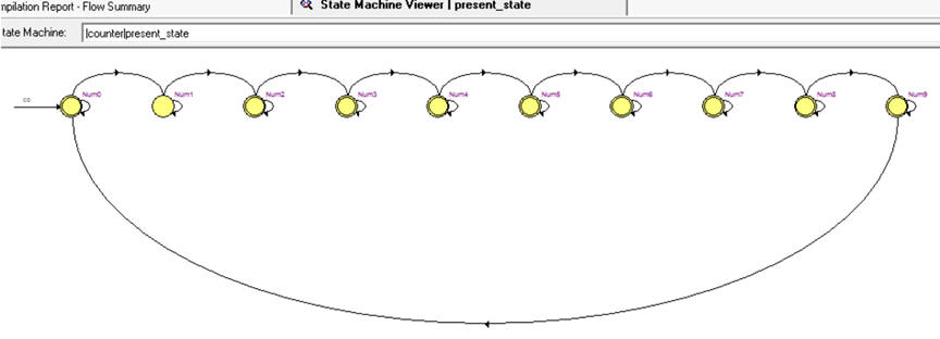
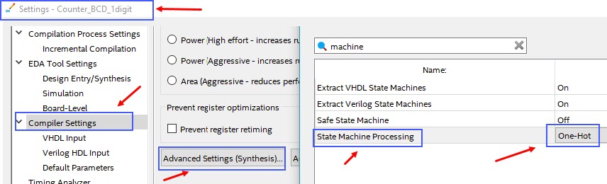
This is the Counter_BCD_1digit.vhd as translated from Fig. 6, 7 and 8. Run the EDA tool to synthesise the circuit and print and comment the RTL schematic using coloured pens. Can you identity each block? Check the number of registers (D_FF) used in the target chip. In this simple example, the answer is 4 if binary sequential coding is selected, or 10 in case of one-hot coding). Fig. 9 shows the state diagram as interpreted by the synthesiser tool.
NOTE: This is the other version of the counter when the truth table is reordered for example considering that CE divides the table in two parts, the loops and the state transitions for counting up.
|
|
| Fig. 9. The state diagram interpreted by the synthesis tool. |
|
|
| Fig. 10. The RTL view using the EDA tool Quartus Prime from Intel. |
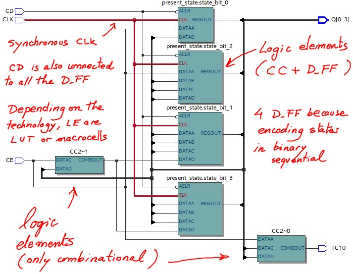
Picture 11 shows the circuit when the states are encoded in binary sequential. Four D_FF are required. Here there is another version of the technology view when the states are encoded in one-hot, thus 10 D_FF are necessary to implement the same counter.
|
|
| Fig. 11. The technology view for a target chip MAX Il EPM2210F324C3 the EDA tool Quartus Prime from Intel. |
4. Testing (functional simulation)
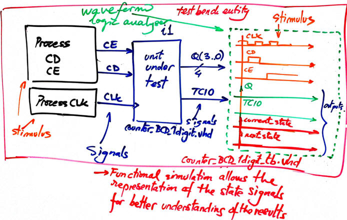
Start the test bench template and add the CLK and inputs activity translating the timing diagram. Thus, to test sequential systems at least two stimulus processes will be required: the CLK and all the other inputs. Make all the timing relative to the CLK_Period constant because this parameter represents the time resolution of the digital system. If a signal is shorter than the CLK period it can not be seen (sampled) or detected (it's a glitch). Consequently, higher time resolutions implies higher CLK frequencies.
|
|
| Fig. 12. The test bench setup showing both, the CLK and other signals stimulus processes. |
This is a sample test bench file counter_BCD_1digit_tb.vhd from which you can copy & adapt the input vectors.
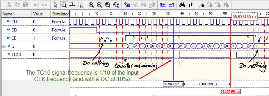
Functional simulation. Run the EDA VHDL tool and demonstrate how the circuit works adding comments to the printed sheet of paper containing the waveforms.
 |
|
|
Fig. 13. Example of a timing diagram to show how the counter works. |
|
5. Testing (gate-level/timed simulations)
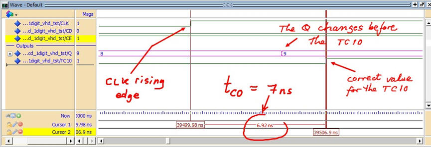
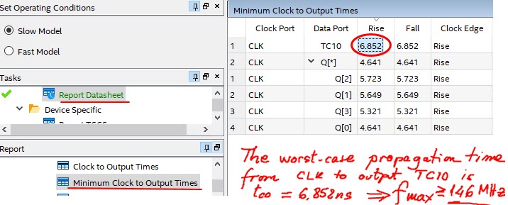
Gate-level simulation. Run the EDA VHDL tool using the same test bench and demonstrate the CLK to output delays and the maximum frequency of operation depending on the technology of the programmable chip use as the target device.
 |
|
|
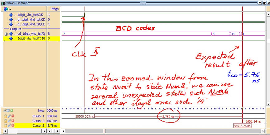
Fig. 14. Example of a timing diagram to show how there is a propagation time CLK to output (tco) fora given target chip (Intel MAX II EPM2210F324C3). |
|
 |
|
|
Fig. 15. In this picture several illegal codes are generated due different propagation times. |
|
 |
|
|
Fig. 16. The worst-case scenario, the maximum operating frequency is calculated using the timing analyser tool. |
|
5. Report
Project report starting with the template sheets of paper, scanned figures, file listings, docx , pptx, or any other resources
6. Prototyping
Use training boards and perform laboratory measurements to verify how the circuit works.
Other materials of interest
- Synchronous counters are basic building blocks of any digital systems, and so, they are documented everywhere. This is the link to the HADES java applets showing many different counters.
 |
Fig. 17. Example of a frequency meter based on the use of a chain of BCD counters to reach a modulo 100000000. |
| Home Term 26/27-Q1 Contact Products Electronic devices and companies Software Books Magazines Instruments DEE Library EETAC DEEL |

|
|
| Web activa des de 09/2001, @ F. J. Robert, Web editat amb Microsoft Expression Web 4. El contingut és un complement als materials d'estudi del curs Circuits i Sistemes Digitals disponibles al campus digital Atenea. Llicència:Reconeixement 4.0 Internacional de Creative Commons |