|
|
Bachelor's Degree in Telecommunications Systems and in Network Engineering |
|
| Analysis and design tutorials | Analysis and design assignments | Prototypes | Exam 1 | Exam 2 | Questions and assessment |
CSD EXA1: midterm exam examples and solution ideas |
2425Q1
Problem 1
1. The ALU_9bit is designed in Lab 4_2. Complete (at least) the 8 lines of the truth table using the given values A and B. The idea of an ALU is discussed in L4.2. This slide below shows how to explain two operations, one of them logic and the other arithmetic. Your aim is to be as clear as possible, as if you had to solve and explain the problem to a large audience repeating procedures and formats found in lectures and examples.
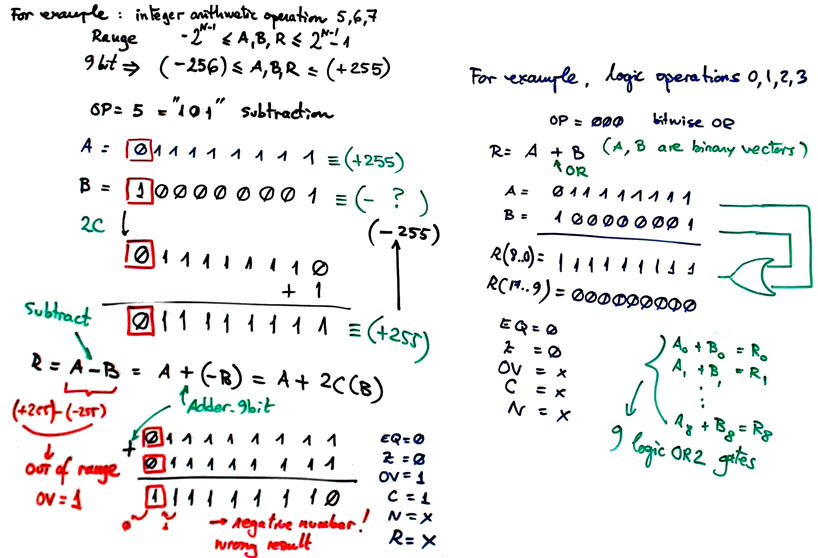
2. An example of a similar Int_Add_Subt_8bit and its internal architecture is presented as the highlighted project P4. L4.1 also explain how to operate integer numbers and the idea of its internal design using components such Adder_8bit.
3. An example of and Adder_1bit using MoD will use a Dec3_8 and two OR gates, as the examples in L3.4. The Adder_1bit is the basic component found in practically all digital systems, it is specified in detail in P3.
4. An example of and Adder_1bit using the MoM is in Lab 3.
Problem 2
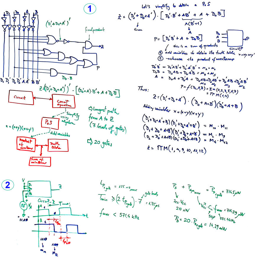
The Circuit_Z is a variation of the highlighted Circuit_C in P1. This "Circuit_Z.pdsprj" is a solution using method II. In the slide below a subcircuit Circuit_P is proposed to infer an intermediate result PoS before expanding Z into a product of maxterms. Alternatively, you can expand the expression Z = (D1' + D0 + A')·(D0'·B' + A + D0·B) to be a SoP and thus deduce the sum of minterms instead.
Problem 3 - Problem 4 - Problem 5 - Problem 6
1. The questions are related to PLA2 circuits: D1.10 (bin - Johnson), D1.10 (Johnson - bin), D1.9, D1.7. Use your reports and feedback to write the answers following exactly our conventions.
2. Plan A equations, strategies (1) - (2) - (3) and (4), are in L1.4 and propagation delay and levels of gates in combinational networks are explained in L4.3. Using canonical sum of minterms or product of maxterms, or minimised SoP or PoS implies 3-levels of gates when the equation is drawn as a logic circuit.
3. How to drive LED is found in L2.4 and basic electrical characteristics in L1.6. Draw the circuit that is driving the LED in the first place, in order to deduce the LED's bias equation and be able to apply values from datasheets.
4. Plan B implies drawing an schematic to show how the full truth table is captured in VHDL, or drawing a flowchart to interpret the truth table sections, as explained in Lab 2 or in many other products solved using this high-level behavioural plan.
| Home Term 26/27-Q1 Contact Products Electronic devices and companies Software Books Magazines Instruments DEE Library EETAC DEEL |

|
|
| Web activa des de 09/2001, @ F. J. Robert, Web editat amb Microsoft Expression Web 4. El contingut és un complement als materials d'estudi del curs Circuits i Sistemes Digitals disponibles al campus digital Atenea. Llicència:Reconeixement 4.0 Internacional de Creative Commons |