

|
Bachelor's Degree in Telecommunications Systems and Network Engineering |

|
Chapter 1 problems |
- D1.7 - |
Multiplexed displays: A: 7-segment |
B: LED bar |
1.- Specifications for the 2-digit multiplexed 7-segment display
We want to use the same 7-segment decoder function for driving multiple common-anode displays. To keep it simple, we implement only a 2-digit multiplexed 7-segment display circuit. In this way, we will multiplex the information to be represented between Digit 1 and Digit 0. As seen in Fig. 1, only one display is active at a given time controlled by input D.
Using the same principle, it is easy to imagine how to expand the circuit for driving a larger number of common-anode 7-segments displays. Thus, this idea on multiplexed display systems or scanning display controllers is generalised in tutorial MDS.
The same project B3.7 is proposed in Chapter 3 for learning the basics of μC software organisation and basic digital I/O.
This Hex_7seg_MUX_2digit.pdsprj simulation in Proteus shows a better idea how the multiplexer works.
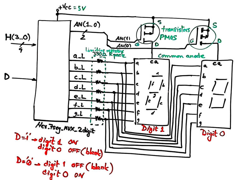 |
Fig. 1. Symbol of Hex_7seg_MUX_2digit. |
Complete the symbol in Fig. 1 and the circuit's truth table in Fig. 2 adding a new input E (enable) that blank the two digits when not active (E = '0').
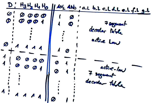 |
Fig. 2. Initial idea of the circuit truth table. |
Draw an example of timing diagram to be used later as stimulus in the VHDL testbench when verifying the synthesised circuit. Consider Min_Pulse = 7.45 ms.
CPLD or FPGA target chip options:
option #1.: MAX II
option #2.: MAX 10 (*)
option #3.: Cyclone IV
(*) MAX10 chips are not used for running gate-level ModelSim simulation because Intel Quartus Prime does not generate the "*.sdo" file accompanying the "*.vho" translation of the technology view. Thus, you can run the timing analyser as usual, and change to another device family for performing examples of gate-level timing diagrams.
How many FPGA resources (logic cells, logic elements, etc.) are used? What is the percentage of the target chip used in this design?
2. Planning
Plan A structural circuit based on logic gates and equations in a single VHDL file. We have many strategies, for instance:
option #1: use minilog to obtain PoS.
In the highlighted project P2 you have an example of an HEX to 7-segment decoder.
Project location:
C:\CSD\P2\Hex_7seg_MUX_2digit_PoS\(files)
Be aware to report these items.
How many FPGA resources (logic cells, logic elements, etc.) are used? What is the percentage of the target chip used in this design?
option #2: use minilog to obtain SoP.
In the highlighted project P2 you have an example of an HEX to 7-segment decoder.
Project location:
C:\CSD\P2\Hex_7seg_MUX_2digit_SoP\(files)
Be aware to report these items.
In the highlighted project P2 you have an example of an HEX to 7-segment decoder.
How many FPGA resources (logic cells, logic elements, etc.) are used? What is the percentage of the target chip used in this design?
Plan B behavioural approach writing the truth table or the high-level description or algorithm in VHDL in a single file (flat).
In the tutorial DT2.6 you can find an example of similar HEX to 7-segment decoder.
Project location:
C:\CSD\P2\Hex_7seg_MUX_2digit_B\(files)
Be aware to report these items.
How many FPGA resources (logic cells, logic elements, etc.) are used? What is the percentage of the target chip used in this design?
After having studied P4 tutorials, additional questions can be added to our report. For instance:
-
Perform a gate-level simulation to measure propagation delays in a given signal transition.
-
Deduce the worst-case propagation delay running the timing analyser tool and calculate the circuit's maximum frequency of operation for the target chip used in the design.
Chapter 1 problems |
- D1.7 - |
Multiplexed displays: A: 7-segment |
B: LED bar |
Design a 28-segment LED bar graph decoder and driver LEDbar_28 capable of displaying in a column format half of the Johnson codes. This device, for different number of LEDs, is widely used in industrial equipment to represent quantities in a vertical scale. For instance, browse these references: 1, 2, 3, 4, 5.
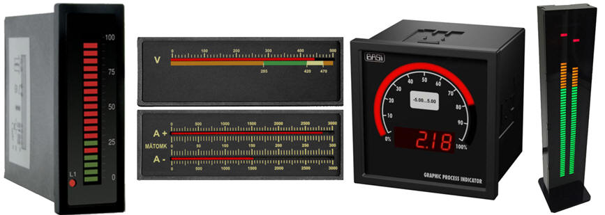 |
Fig. 1. Pictures of LED bar indicators. |
This device is also used in professional audio equipment as a volume-unit meter (VU-meter).The reading of the volume indicator is 0 VU (or +4 dBm) when it is connected to a 1.228 VRMS 1 kHz sinusoidal waveform driving a 600 Ω load.
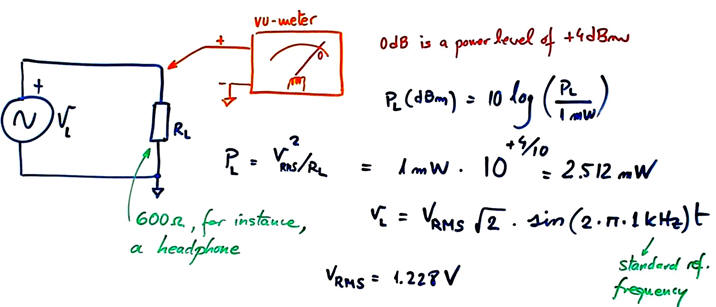 |
Fig. 2. Vu-meter scale and power levels. |
Furthermore, the VU-meter scale employs a logarithmic distribution. For example, a -10 dB indication corresponds to a power level of +4 dBm - 10 dB = -6 dBm (251.2 µW), or a load voltage of 388.2 mVRMS. The LM3916 integrated circuit by Texas Instruments emulates the precise ballistic characteristics of classical mechanical needle meters, providing discrete steps at -20, -10, -7, -5, -3, -1, 0, +1, +2, and +3 dB. A comparable alternative is the BA682A from ROHM.
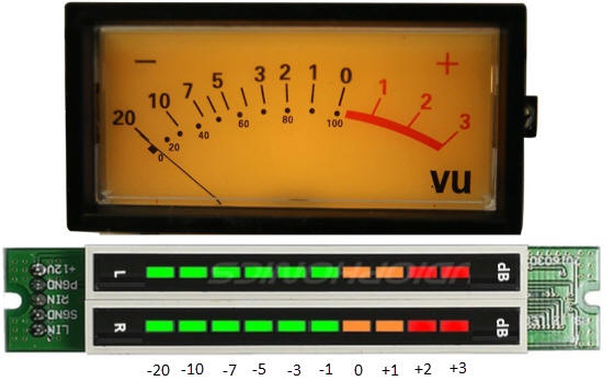 |
Fig. 3. Example of a classic analogue VU-meter and its digital equivalent in 10-LED column. |
1.- Specifications for the 28 LED bar
- 28 LED segments column type BL28-3005SK04Y, common cathode, driven by a binary to one-hot decoder combinational circuit Bar_28LED_dec. The idea of such a structure is to save pins simplifying the hardware interface: 11 outputs instead of 28. In the same way we can think of a similar device to drive 60 LEDs to indicate the seconds sphere in a wall clock.
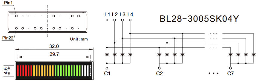 |
Fig. 4 LED bar common cathode internal connections. |
- Multiplexed display system MDS_LEDbar28 to display from binary (0 ≤ B ≤ 28) to Johnson ("00 ... 00", "10 ... 00", ..., "110 ... 00", "11 ... 10", "11 ... 11") using a programmable Counter_mod29 (to be designed in P7).
- 5-bit radix-2 to 7-segment decoder to represent tens and units.
- Proteus simulation file "LED_bar_28.pdsprj" illustrates the approach for driving the LED column via a combinational logic circuit. To ensure correct operation at the required LED bias point, MOS transistors are integrated as driving elements.
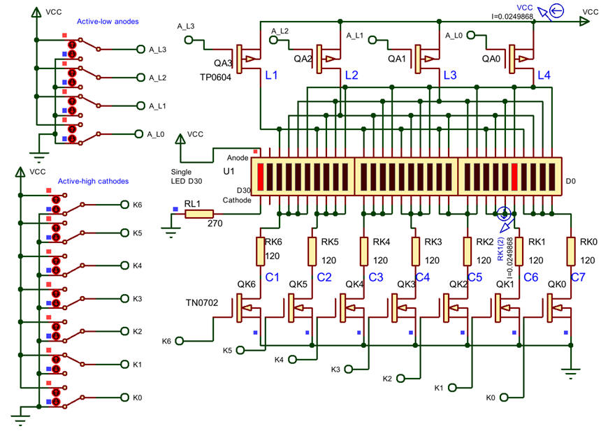 |
Fig. 5. Proteus simulation to experiment with the LED bar and determine which A_L and K values are required to light each LED. |
The symbol for the complete application is shown in Fig. 6. We will enhance the circuit with 7-segment outputs to represent along with the LED column, the tens and units in binary-coded decimal (BCD). For instance, a radix-2 input "00110" lights six column LEDs and shows "06".
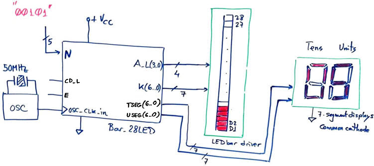 |
Fig. 6. Symbol of LED_bar_28. |
Fig. 7 proposes a complete internal architecture for this component, which also requires circuits described in Chapter 2 (Chip5 and Chip6). To obtain a column Johnson code visualization, the complete circuit requires a programmable binary down-counter to generate the number of bars to be illuminated and a decoder to convert from binary radix-2 to one-hot encoding. Additionally, the scanning frequency must be specified—for instance, 60 Hz when illuminating the full bar without flicker. Each code sequence has a duration of TC = 575 µs, which corresponds to a clock frequency fCLK = 1.74 kHz.
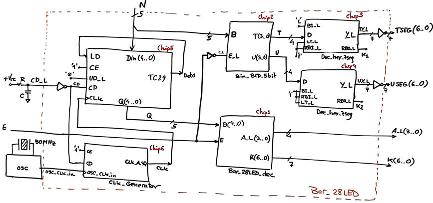 |
Fig. 7. Bar_28LED internal architecture. |
Complete the Bar_28LED_dec combinational circuit (Chip1) truth table in Fig. 8. The input E (enable) will blank the bar, as it happens with B = 0, when not active for E = '0'.
The same project B3.7 is proposed in Chapter 3 for learning the basics of μC software organisation and basic digital I/O.
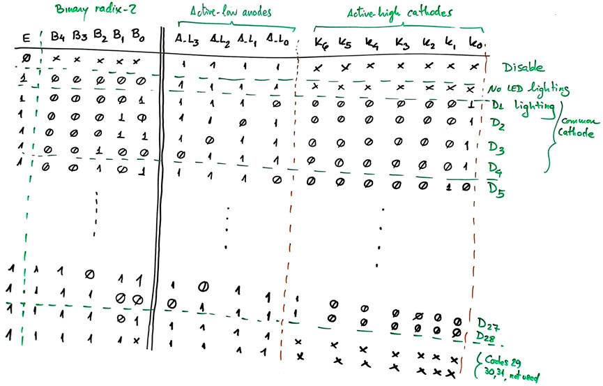 |
Fig. 8. Initial idea of the Bar_28LED_dec truth table. The code conversion is from binary radix-2 to one-hot in a way that only one LED is activated at a time. Therefore, to visualise a Johnson column code lighting up to the LED N, it is necessary to apply at high speed all the codes from 0 ≤ B ≤ N. This is the mission of the Counter_mod29. |
Draw an example of timing diagram to be used later as stimulus in the VHDL testbench when verifying the synthesised circuit. Consider Min_Pulse = 575 µs.
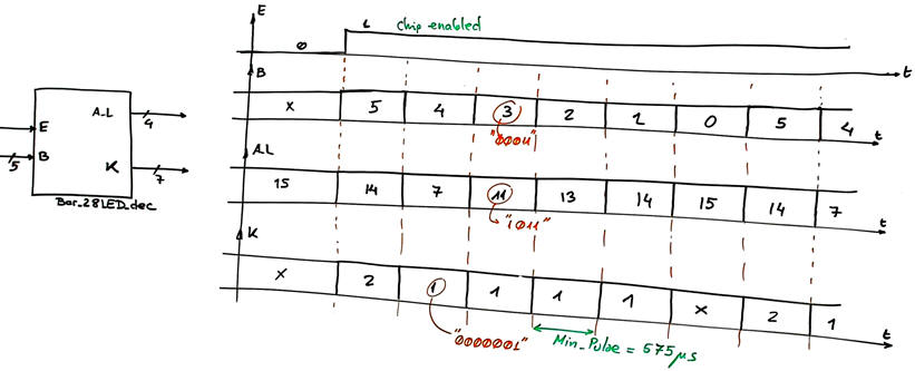 |
Fig. 9. Example timing diagram for testing Chip1. It may the translated to a VHDL testbech. |
CPLD or FPGA target chip options:
option #1.: MAX II
option #2.: MAX 10 (*)
option #3.: Cyclone IV
(*) MAX10 chips are not used for running gate-level ModelSim simulation because Intel Quartus Prime does not generate the "*.sdo" file accompanying the "*.vho" translation of the technology view. Thus, you can run the timing analyser as usual, and change to another device family for performing examples of gate-level timing diagrams.
How many FPGA resources (logic cells, logic elements, etc.) are used? What is the percentage of the target chip used in this design?
2. Planning
Plan A: Structural circuit based on logic gates and equations in a single VHDL file. We have many strategies, for instance:
option #1: use minilog to obtain PoS.
In the highlighted project P2 you have an example of an HEX to 7-segment decoder.
Project location:
C:\CSD\P2\Bar_28LED_dec_PoS \(files)
Be aware to report these items.
How many FPGA resources (logic cells, logic elements, etc.) are used? What is the percentage of the target chip used in this design?
option #2: use minilog to obtain SoP.
In the highlighted project P2 you have an example of an HEX to 7-segment decoder.
Project location:
C:\CSD\P2\Bar_28LED_dec_SoP\(files)
Be aware to report these items.
In the highlighted project P2 you have an example of an HEX to 7-segment decoder.
How many FPGA resources (logic cells, logic elements, etc.) are used? What is the percentage of the target chip used in this design?
Plan B: Behavioural approach writing the truth table or the high-level description or algorithm in VHDL in a single file (flat).
In the tutorial DT2.6 you can find an example of similar HEX to 7-segment decoder.
Project location:
C:\CSD\P2\Bar_28LED_dec_B\(files)
Be aware to report these items.
How many FPGA resources (logic cells, logic elements, etc.) are used? What is the percentage of the target chip used in this design?
Plan C2: We will begin by addressing the Chapter 1 circuits shown in the Fig. 10 symbol. Design and test the top-level LED_bar_28 architecture, which consists of the combinational circuits Chip1, Chip2, Chip3, and Chip4. Identify and adapt suitable components from our tutorials.
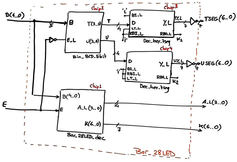 |
Fig. 10. Combinational section of the top architecture. |
Project location:
C:\CSD\P3\Bar_28LED\(files)
Be aware to report these items.
How many FPGA resources (logic cells, logic elements, etc.) are used? What is the percentage of the target chip used in this design?
How many VHDL files contains this project?
After having studied P4 tutorials, additional questions can be added to our report. For instance:
-
Perform a gate-level simulation to measure propagation delays in a given signal transition.
-
Deduce the worst-case propagation delay running the timing analyser tool and calculate the circuit's maximum frequency of operation for the target chip used in the design.
NOTE (optional): This project can be continued in P7 and P8 to design the remaining sequential blocks Counter_mod29 and CLK_Generator circuit proposed in Fig 7. A final top prototype may be built on a DE10-Lite platform.
| Home Term 26/27-Q1 Contact Products Electronic devices and companies Software Books Magazines Instruments DEE Library EETAC DEEL |

|

|
| Web activa des de 09/2001, @ F. J. Robert, Web editat amb Microsoft Expression Web 4. El contingut és un complement als materials d'estudi del curs Circuits i Sistemes Digitals disponibles al campus digital Atenea. Llicència:Reconeixement 4.0 Internacional de Creative Commons |