|
|
Bachelor's Degree in Telecommunications Systems and in Network Engineering |
|
P1: analysis of simple circuits based on logic gates |
| Resources in lectures and labs: | L1.1, L1.2, L1.3, Lab1.0, Lab1.1, Lab1.2 | Project | objectives |
Highlighted tutorial analysis project: Circuit_C
| Method I | Method II | Method III | Method IV |
| 1. Specifications | Planning | Developing | Testing | Report |
Deduce the truth table of Circuit_C in Fig. 1 using analysis method I and compare and discuss solutions.
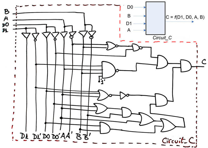 |
| Fig. 1. Example Circuit_C to analyse. |
We will organise our analysis projects using four sections as indicated in Fig. 2.
 |
| Fig. 2. Organise your analysis project following this sequence. Write your report only when your result is verified using another analysis method, which is another complete project for the same circuit. |
Fig 3 shows the general concept map including up to four methods for analysing simple combinational circuits.
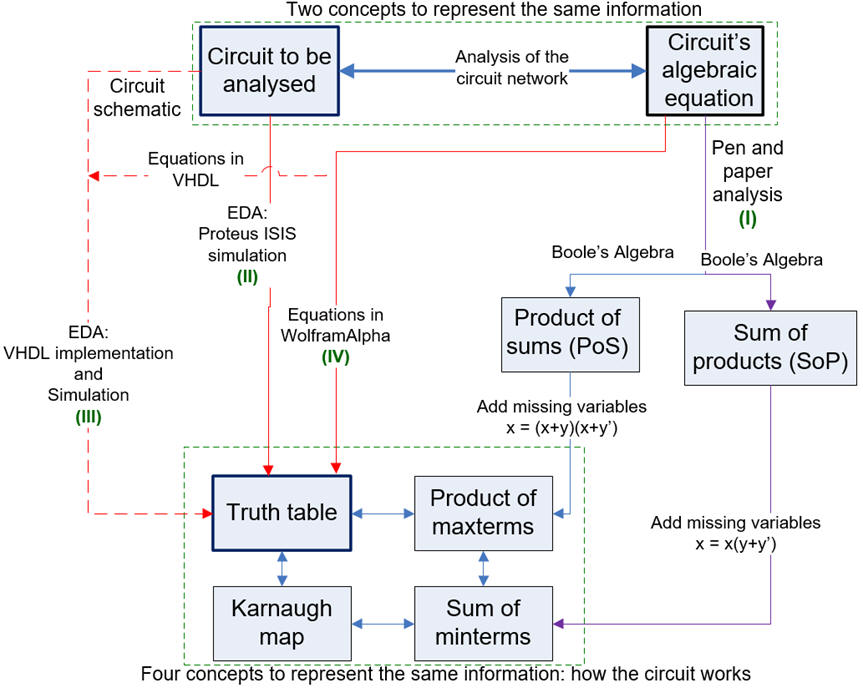 |
| Fig. 3. Proposed analysis methods (Visio). The concept map combining analysis and design (Visio). |
These are other tutorial analysis and assignments.
NOTE: designing circuits from a given truth table is discussed and proposed in the next complementary P1 design page.
| Specifications | 2. Planning | Developing | Testing | Report |
Analytical method using Boolean algebra and pen & paper. If the circuit is too large or you are still a beginner, it is better to start solving only a section of the circuit.
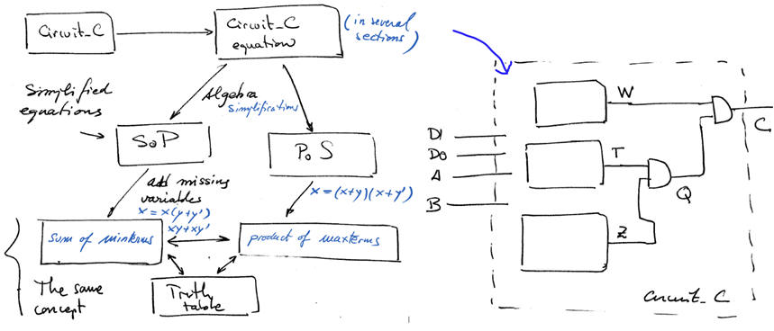 |
| Fig. 4. Planning method I subdividing the circuit in sections. |
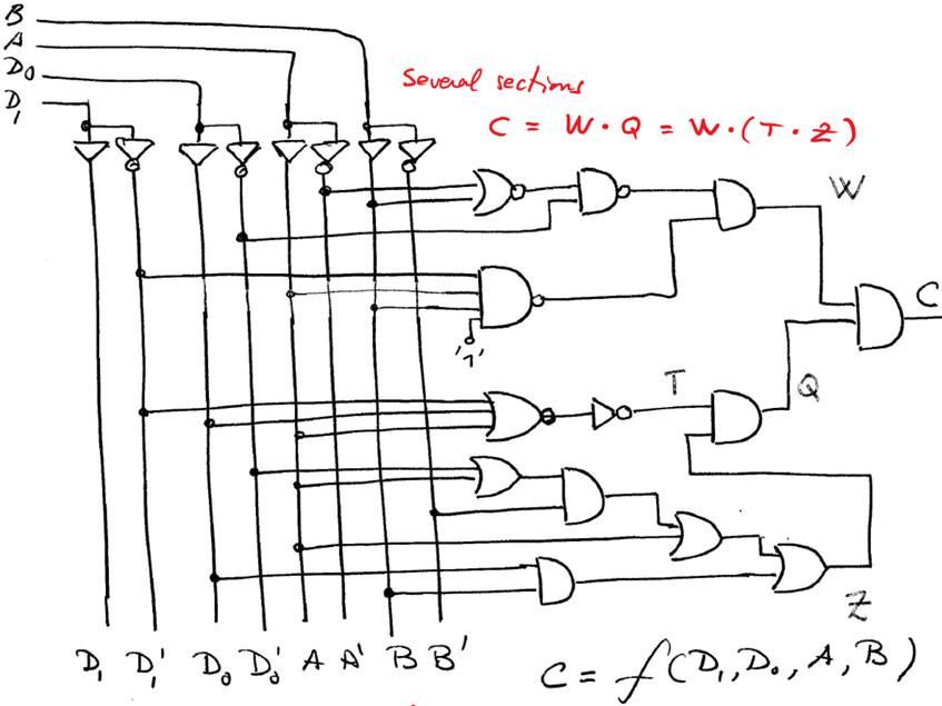
Find the circuit equation.
Simplify equations until simple SoP or PoS equations are obtained.
Add missing variables to convert SoP into sum of minterms or PoS into product of maxterms.
Project location for saving pictures, scanned sheets of paper, etc...
C:\CSD\P1\Circuit_C\algebra\(files)
| Specifications | Planning | 3. Developing | Testing | Report |
Handwritten analysis of Circuit_C and rec.
 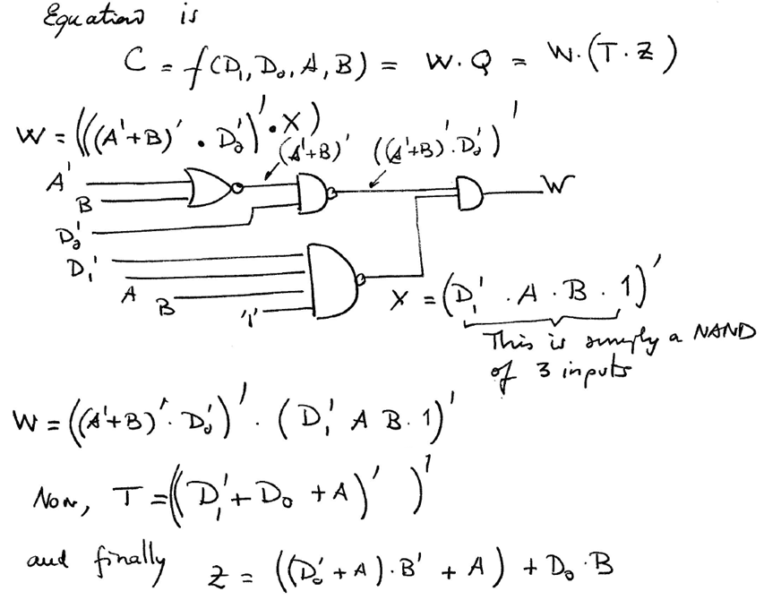  |
| Fig. 5. Deducing the circuit's equation. |
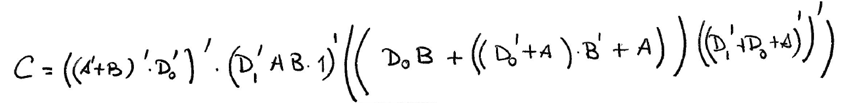
We can apply algebra to the general circuit equation in Fig. 5, to try to simplify it and obtain a simpler equation in PoS or SoP format.
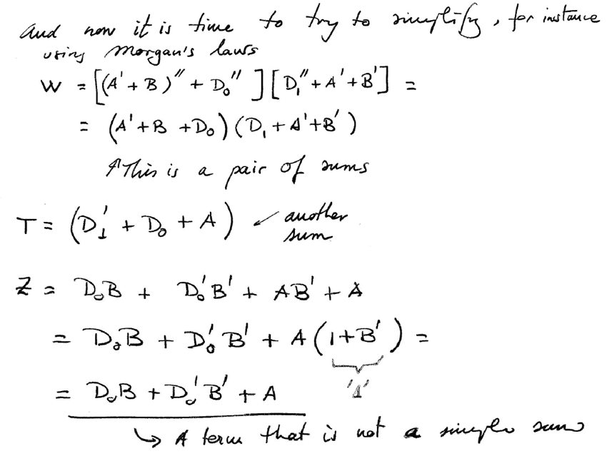 |
| Fig. 6. Simplification using algebra. |
Term Z is complicated, because is not a simple sum or a product. Thus, we can imagine the equation as another independent subcircuit Z = f(D0, A, B):
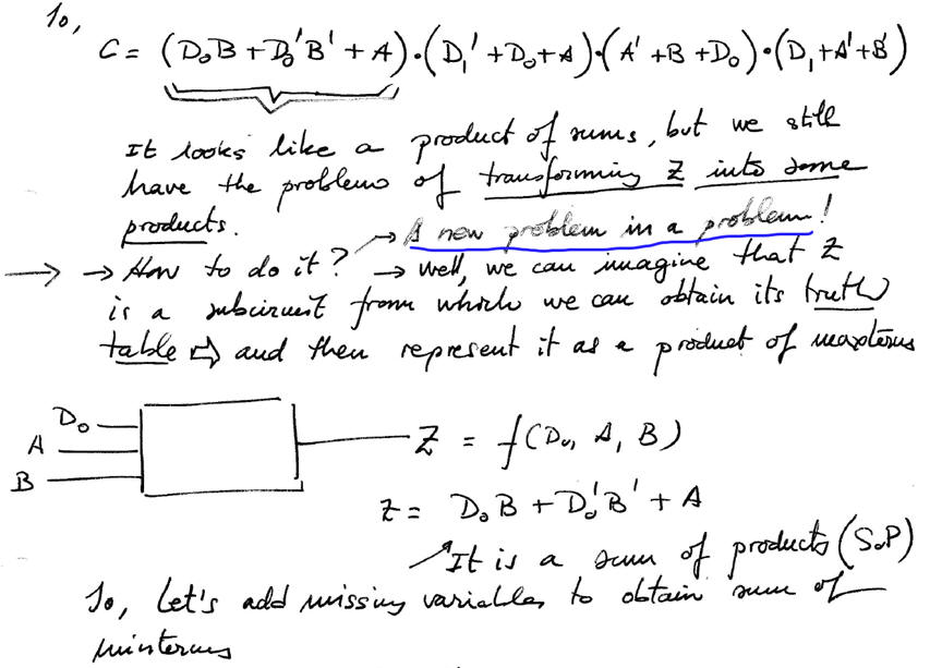 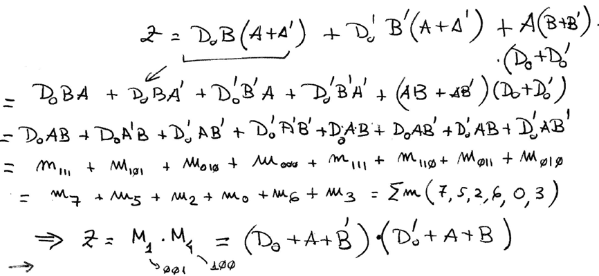 |
| Fig. 7. Analysis of Circuit Z = f(D0, A, B). |
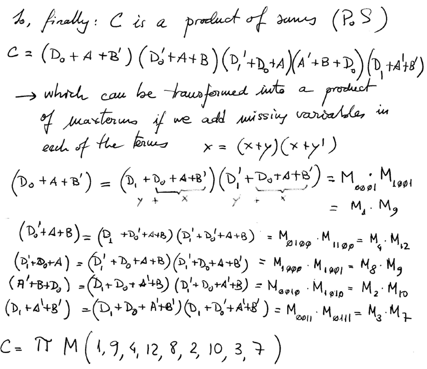  |
| Fig. 8. Final equations that we have to compare with results from other methods. |
| Specifications | Planning | Developing | 4. Testing | Report |
Testing means to check or verify that the solution is correct and agrees with the initial specifications.
In this analysis section, the simplest way to check the truth table is by comparison with the truth table obtained by other methods.
| Specifications | Planning | Developing | Testing | 5. Report |
Project report: sheets of paper, scanned and annotated figures, file listings, notes or any other resources. In CSD follow this rubric of indications for writing reports.
| Method I | Circuit_C method II | Method III | Method IV |
| 1. Specifications | Planning | Developing | Testing | Report |
Deduce the truth table of Circuit_C in Fig. 1 using analysis method II and compare and discuss solutions.
|
|
| Fig. 1. Example Circuit_C to analyse. |
| Specifications | 2. Planning | Developing | Testing | Report |
Planning means organising and discussing how to proceed to reach solutions. A flow chart of sequential operations will be necessary to explain what to do, how to do it and when.
- Choose Proteus as circuit simulator: draw/capture the circuit schematic in Proteus and run a simulation.
- In CSD we never start a project or a simulation from scratch, but we copy and adapt from similar exercises found here in this digsys web. For example, use files to copy and adapt from Lab 1.1.
- Select a library of a classic technology, for instance LS-TTL or CMOS series 4000.
- Try all the possible input combinations to fill in and complete the truth table.
Project location:
C:\CSD\P1\Circuit_C\Proteus\(files)
| Specifications | Planning | 3. Developing | Testing | Report |
Developing means executing a given plan to achieve a circuit solution. Fig. 2 shows an example of Proteus capture for Circuit_C.pdsprj
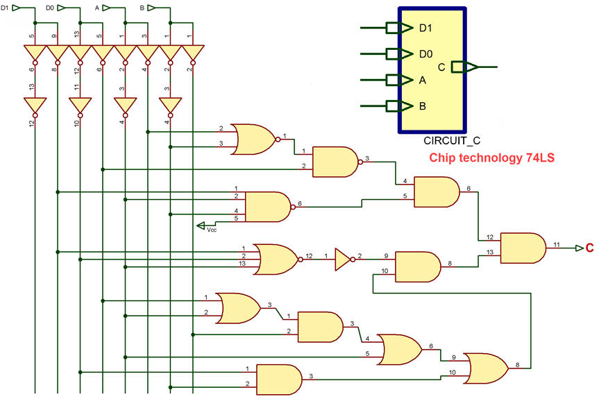 |
Fig. 2. Circuit_C captured in Proteus ready for running simulations. |
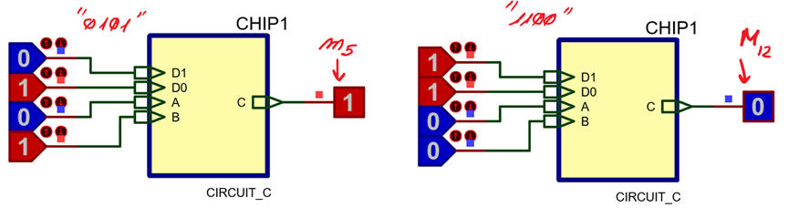
Pictures in Fig. 3 show interactive simulation results for two of the sixteen combinations.
|
|
|
Fig. 3. Simulation results when applying input binary combinations "0101" and "1100". We can observe that "0101" generates minterm m5 and "1100" generates maxterm M12. |
In this way, trying all 16 combinations we reach the final truth table:

| Specifications | Planning | Developing | 4. Testing | Report |
Testing means to check or verify that the solution is correct and agrees with the initial specifications.
In this analysis section, the simplest way to check the truth table is by comparison with the truth table obtained by other methods.
| Specifications | Planning | Developing | Testing | 5. Report |
Project report: sheets of paper, scanned and annotated figures, file listings, notes or any other resources. In CSD follow this rubric of indications for writing reports.
| Method I | Method II | Circuit_C Method III | Method IV |
| 1. Specifications | Planning | Developing | Testing | Report |
Deduce the truth table of Circuit_C in Fig. 1 using analysis method III and compare and discuss solutions.
|
| Fig. 1. Example Circuit_C to analyse. |
| Specifications | 2. Planning | Developing | Testing | Report |
VHDL synthesis and simulation project.
- Translate to VHDL Circuit_C algebraic equation in Fig. 5 using a similar file to copy and adapt.
- Choose a target chip, for instance CPLD MAX II EPM2210F324C3, and start a VHDL synthesis project using an EDA tool, for instance Quartus Prime.
- Examine and print the RTL and technology schematics.
- Start a VHDL simulation project, for instance in ModelSim-Intel FPGA Starter Edition, using a testbench to input signal stimulus .
Project location:
C:\CSD\P1\Circuit_C\VHDL\(files)
| Specifications | Planning | 3. Developing | Testing | Report |
This is an example of Circuit_C.vhd translated to VHDL to synthesise the circuit.
This is an example Circuit_C_tb.vhd VHDL testbench to obtain the circuit's truth table.
 |
Fig. 2. Example RTL (register transfer level) ideal schematic from Quartus Prime synthesiser. |
 |
| Fig. 3. Truth table deduced from the simulation of all the input test vectors. |
| Specifications | Planning | Developing | 4. Testing | Report |
Testing means to check or verify that the solution is correct and agrees with the initial specifications.
In this analysis section, the simplest way to check the truth table is by comparison with the truth table obtained by other methods.
| Specifications | Planning | Developing | Testing | 5. Report |
Project report: sheets of paper, scanned and annotated figures, file listings, notes or any other resources. In CSD follow this rubric of indications for writing reports.
| Method I | Method II | Method III | Circuit_C method IV |
| 1. Specifications | Planning | Developing | Testing | Report |
Deduce the truth table of Circuit_C in Fig. 1 using analysis method IV and compare and discuss solutions.
|
| Fig. 1. Example Circuit_C to analyse. |
| Specifications | 2. Planning | Developing | Testing | Report |
Numerical engine WolframAlpha to be used for inferring the truth table from the circuit's algebraic equation.
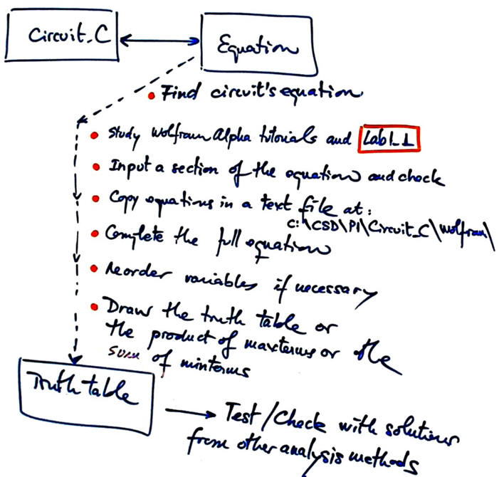 |
Fig. 2. Planning the method IV as a bullet list of operations. |
- Write the circuit equation in Fig. 1 in a text file step-by-step.
- Use files to copy and adapt them from Lab 1.1. or WolframAlpha.
- Reorder input variables if such is the case before annotating maxterms and minterms.
- Draw the truth table.
- Project location:
C:\CSD\P1\Circuit_C\wolfram\(files)
| Specifications | Planning | 3. Developing | Testing | Report |
Circuit and equation are at the same conceptual level.
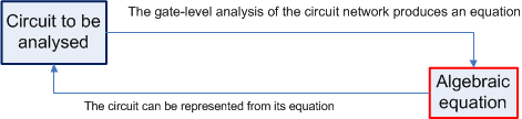 |
Fig. 3 Circuit equation. |
|
|
This is an example Circuit_C_equation.txt file to be pasted in WolframAlpha window. And Fig. 4 shows results from WolframAlpha engine.
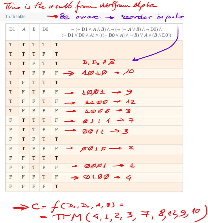 |
| Fig. 4. Results from WolframAlpha representing the truth table. Be aware of reordering the input variables. |
| Specifications | Planning | Developing | 4. Testing | Report |
Testing means to check or verify that the solution is correct and agrees with the initial specifications.
In this analysis section, the simplest way to check the truth table is by comparison with the truth table obtained by other methods.
| Specifications | Planning | Developing | Testing | 5. Report |
Project report: sheets of paper, scanned and annotated figures, file listings, notes or any other resources. In CSD follow this rubric of indications for writing reports.
6. Prototyping
Any of our circuits can be built as a prototype for laboratory experimentation, measurements and characterisation. We will use, for instance, the Terasic DE10-Lite board as explained in Lab1.2. The VHDL architecture of Circuit_C synthesised in the FPGA will contain the circuit's algebraic equation.
| Home Term 26/27-Q1 Contact Products Electronic devices and companies Software Books Magazines Instruments DEE Library EETAC DEEL |

|
|
| Web activa des de 09/2001, @ F. J. Robert, Web editat amb Microsoft Expression Web 4. El contingut és un complement als materials d'estudi del curs Circuits i Sistemes Digitals disponibles al campus digital Atenea. Llicència:Reconeixement 4.0 Internacional de Creative Commons |