|
|
Bachelor's Degree in Telecommunications Systems and in Network Engineering |
|
P4: arithmetic operations for signed integers in 2C. Measuring propagation delay and circuit speed |
| Resources in lectures and labs: | L4.1, LAB4.1, LAB4.2, L4.2, L4.3 | Project | objectives |
Highlighted project: 8-bit adder-subtractor for signed integers. How fast is this circuit?
| 1. Specifications | Planning | Developing | Functional test | Gate-level test | Report | Prototype |
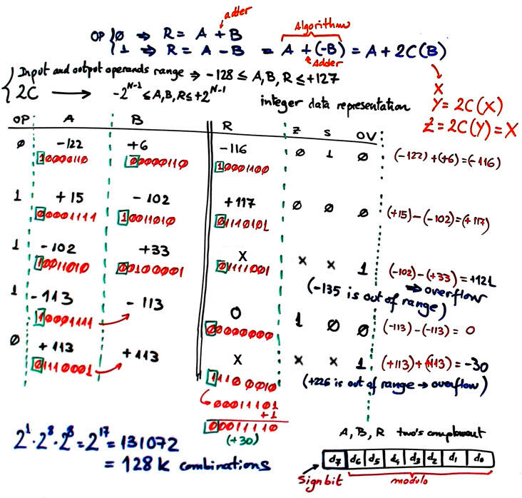
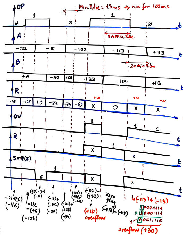
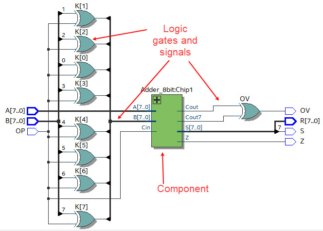
[A]. Design an 8-bit adder and subtractor in two's complement with zero (Z), sign (S) and overflow (OV) flags using VHDL and multiple-file hierarchical structural approach (plan C2). Discus the symbol (below in Fig 1). Write its truth table. How long is it? Draw a timing diagram example and perform several operations in 2C to learn how the circuit will work.
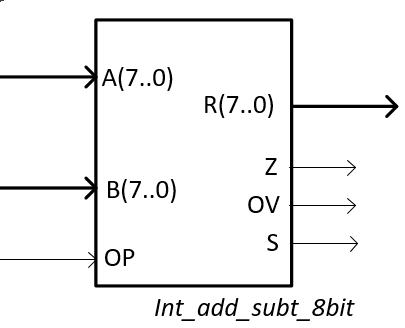 |
Fig. 1. a) Symbol of an 8-bit two's complement (2C) adder-subtractor. Run this project solved in Proteus Int_add_subt_8bit.pdsprj and try to visualise better how operates and how the two's complemented data looks like. Accompany the truth table and the timing diagram operating in binary 2C some examples using the circuit's algorithm. |
 |
|
| b) Example of truth table combinations. Int_add_subt_8bit works with signed integer operands. When the OV flag is asserted for a given operation, neither the result or the other flags have interest (don't' care). |
|
  |
|
c) Timing diagram sketch showing how the Int_Add_Subt_8bit performs several additions and subtractions in time using two's complement signed integer operands. This sketch is ready for translation as a VHDL testbench stimulus process below at the test section. |
|
[B]. Circuit's maximum processing speed. Once the circuit works and is tested functionally as usual (design sections #1 - #2 - #3 - #4), perform in a new design section #5 a gate-level simulation to determine the circuit's propagation delay in a given transition and also the circuit's maximum speed of operation using the timer analyser tool.
VHDL design flow shows gate-level simulation as the 5th design step before making real measurements in the lab uploading the configuration file to the prototyping board. For instance, two different experiments can be carried out:
|
|
Other design tutorials and assignments.
| Specifications | 2. Planning | Developing | Functional test | Gate-level test | Report | Prototype |
We can deduce the plan for this circuit studying the algorithm behind results and flags. The idea is to use for both, additions and subtractions, the Adder_8bit for radix-2 numbers studied in LAB3.
XOR gate as programmable Buffer/NOT gate
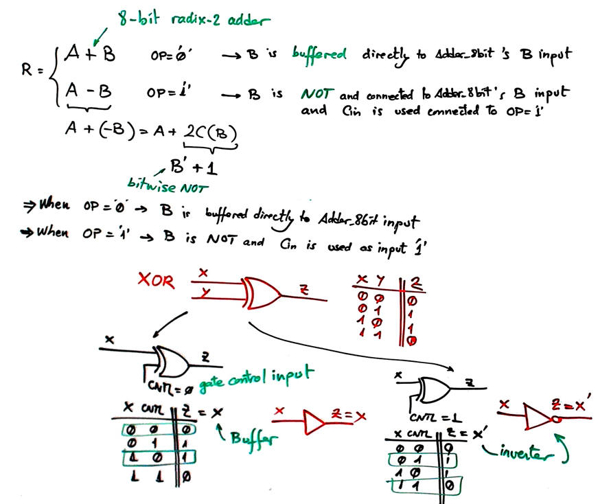 |
| Fig. 2. XOR gate examined as a configurable NOT or buffer. |
Zero detector flag
Study how the zero flag (Z) works. Is it the same as in Adder_8bit? (Int_add_subt_8bit Z flag does not include Cout signal)
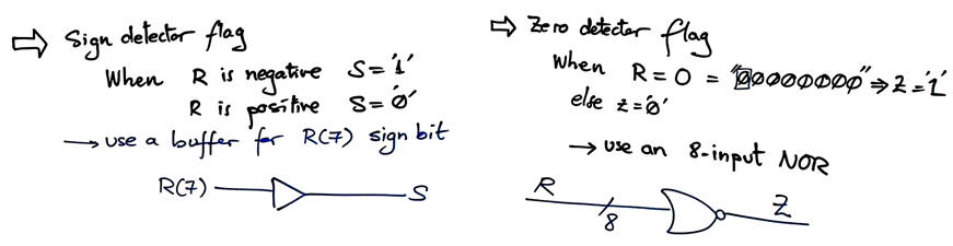 |
Fig. 3. Circuits for sign (S) and zero (Z) flags. If Adder_4bit from P3 is to be used, we have to modify it, so that Z equation is not including Cout, thus: Z = (Y3 + Y2 + Y1 + Y0)' |
Overflow flag
Study how the overflow logic (OV) works and how a circuit can be inferred.
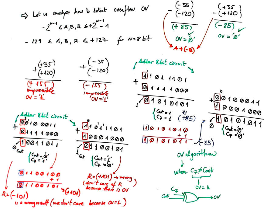 |
Fig. 4. On the detection of the overflow condition. Carry C7 has to be made available from the Adder_8bit. |
Another algorithm for detecting overflow situations, specially indicated when the inner carry C7 is not available is described in this book slides (chapter 10): Ercegovac, M., Lang, T., Moreno, J. H., Introduction to digital systems, John Wiley & Sons, 1999. When operands A, B have different sign there is never overflow; when both operands A, B have the same sign and the result a different sign, there is an overflow situation. Translated to an equation paying attention to the three sign bits:
OV = A7' · B7' · Q7 + A7 · B7 · Q7'
Optimised integer adder and subtractor
The final plan C2 for the Int_add_subt_8bit is represented in Fig. 5.
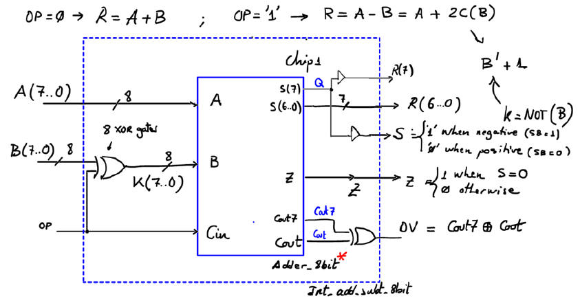 |
| Fig. 5. Proposed plan. |
Count and name all the components and VHDL files involved in the project. For instance, the Adder_8bit can be based on the ripple-carry technique (option #1: RC). or carry-lookahead (option #2: CLA).
Complete your schematics studying and adapting the component Adder_4bit to generate the modified version of the Adder_8bit for radix-2 number required in Fig. 5 as Chip1.
Project folder location:
C:\CSD\P4\Int_add_subt_8bit\(files) /p>
| Specifications | Planning | 3. Developing | Functional test | Gate-level test | Report | Prototype |
Once you have completed the planning of the several layers of the project in Fig. 5, you can start the synthesis process. Write down the VHDL files translating the plans above using components and signals modifying a convenient seed circuit. For instance, these circuits may suit you: Adder_1bit.vhd, Adder_4bit.vhd, Adder_8bit.vhd, Int_add_subt_8bit.vhd. You see that the 4-bit and 8-bit adders are slightly modified because the overflow flag OV is generated using the two most significant carry signals.
Run the EDA tool to synthesise the circuit. Print and comment the RTL schematic. Verify that Fig. 6 is like what you had sketched in the plan.
 |
| Fig. 6. Example of RTL diagram schematic interpreted by the EDA synthesis tool. |
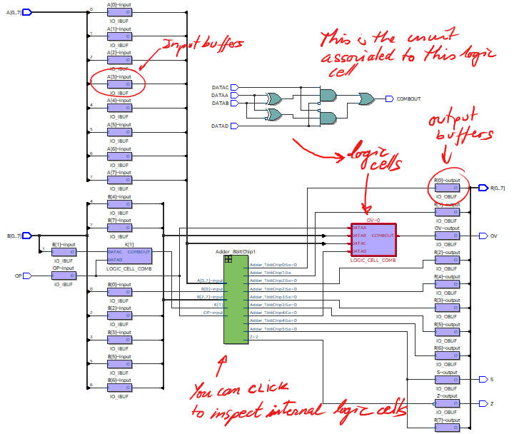
At this level, it is very interesting for you to play with technology schematics as well. They are the real synthesised circuits for a given target chip. In addition to the technology view, there is also the chip planner tool where you can locate exactly the logic cells used in the design.
|
| Fig. 7. Example of technology implementation in an FPGA Cyclone IV EP4CE115F29C7 (option #2) from Intel. In this example circuit, 21 logic elements are used of the 114480 available. Remark how no memory registers/latches are used because it is a combinational circuit (Chapter I) instead of a sequential system (Chapter II). In this sense, if your implementation contains registers or inferred latches it means that it is wrong and you must debug your architecture to find mistakes in VHDL files. |
| Specifications | Planning | Developing | 4. Functional test | Gate-level test | Report | Prototype |
The testbench fixture containing the main ideas and concepts involved in this schematic is represented in Fig. 8.
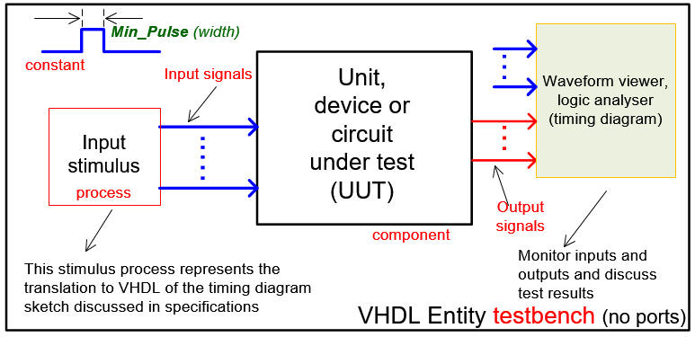 |
| Fig. 8. Testbench VHDL schematic. |
Generate a testbench template from Quartus Prime. Rename and move it to the project folder. Delete the empty stimulus process.
Convert the initial timing diagram sketch in Fig. 1c into a VHDL testbench. For example, copy only the stimulus process and the constant Min_Pulse from this file: Int_add_subt_8bit_tb.vhd. Use several positive and negative integer numbers as inputs. Test both additions and subtractions. Check overflow and zero situations.
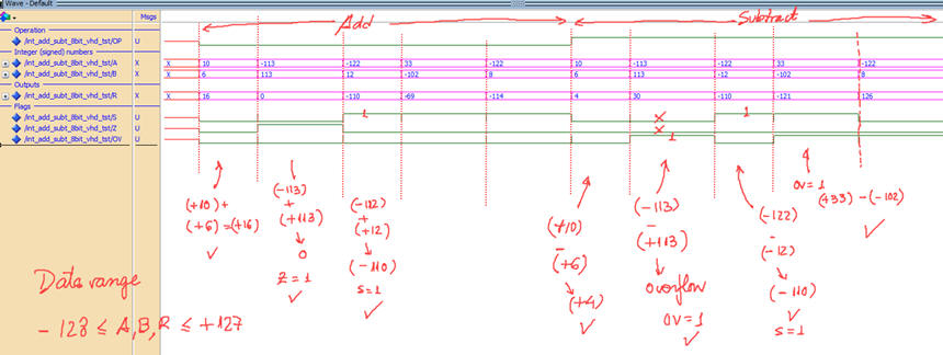
Run the EDA VHDL simulator and demonstrate how the circuit works adding comments to the printed sheet of paper containing the waveforms, as shown in Fig. 9.
 a) 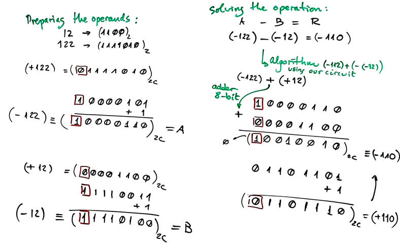
|
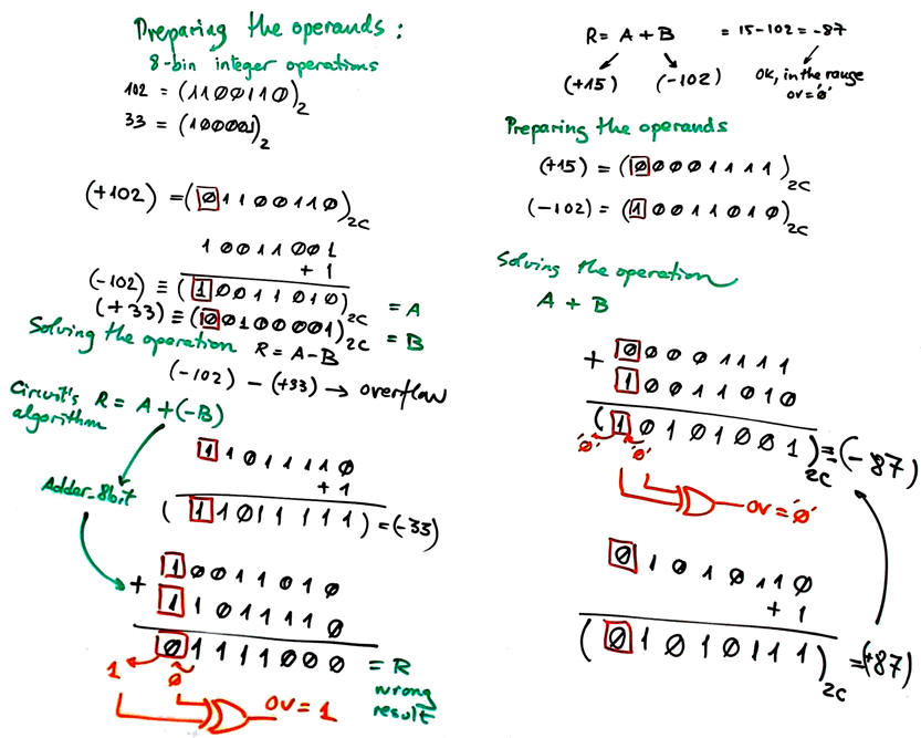
Fig. 9. a) Example test waveform diagram with some input vectors. A, B and R are 2C numbers. In ModelSim select "radix decimal" to identify correctly the binary numbers as signed integers. b) To verify your results and get some practice, you better calculate several operations in paper using binary symbols, this is how the circuit calculates (-112) - (-12) = (-110). You can also run our Proteus project Int_add_subt_8bit.pdsprj to visualise how the circuit operates and how the integer numbers in two's complemented look like. |
| Specifications | Planning | Developing | Functional test | 5. Gate-level test | Report | Prototype |
Two tools for dynamic characterisation: gate-level ModelSim simulations and Quartus Prime timing analyser.
Gate-level simulations
Run a gate-level simulation to measure the worst case delay and the maximum speed of operation (or highest computation speed) of the synthesised circuit. You can practice as well these new tools running the LAB4 tutorial circuits.
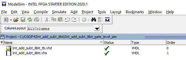
Fig. 10 shows the new simulation project, considering the testbench and the flat technology view schematic translated to VHDL by Quartus Prime as the Int_Add_Subt_8bit.vho file.
|
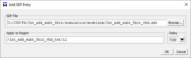
Fig. 10. Gate-level project files. Attach the SDF file to the simulation. |
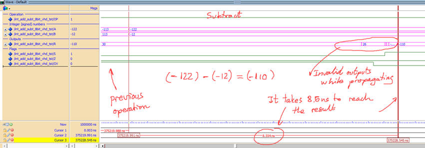
Perform gate-level simulations on several input vectors examining (zooming in) signal transitions. Measure the circuit propagation delay.
|
Fig. 11. Example waveform for the Int_add_subt_8bit showing how the opeartion (-122) - (-12) = (-110) is computed over time generating wrong results until all signals have propagated through the circuit. Target chip: Cyclone IV FPGA EP4CE115F29C7. |
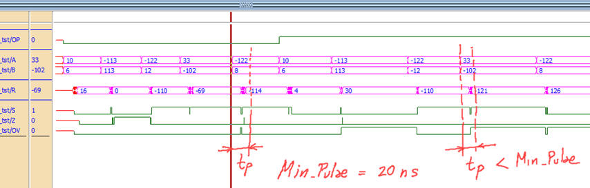
When Min_Pulse constant is similar to propagation times the circuit cannot produce correct results.
a) 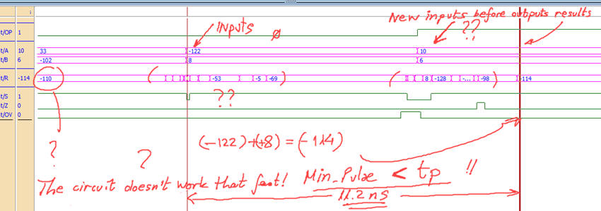
b) |
Fig. 12. (a) Results for Min_Pulse = 20 ns, the circuit still operating correctly. (b) Results for Min_Pulse = 8 ns, too fast, new input stimulus is applied before the circuit sets the outputs of the previous operation. |
Timing analyser
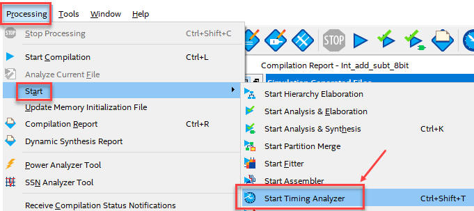
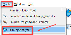
Use the Quartus Prime timing analyser tool to determine the longest propagation delay path from inputs to outputs (worst-case scenario), and thus the maximum speed for calculating 8-bit integer additions and subtractions for a given target chip. For instance, considering Intel chips, which is faster, MAX II CPLD EPM2210F324C3 or Cyclone IV FPGA EP4CE115F29C7N ?
 |
|
|
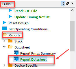 |
Fig. 13. Processing the timing analyser spreadsheet engine and reporting datasheet results. |
|
As shown in Fig. 14, switching OP from H to L (falling edge) and waiting for setting the Z flag from H to L (falling edge), generates the maximum propagation delay tP = 14.691 ns.
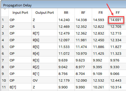 |
Fig. 14. A section of the timing analyser spreadsheet showing the worst-case scenario. |
Therefore, if input OP has a switching period T, its minimum value is Tmin = 2·tP = 29.34 ns. In this circuit the maximum speed is fMAX < 34 MHz (34 millions of operations per second).
| Specifications | Planning | Developing | Functional test | Gate-level test | 6. Report | Prototype |
It is required a handwritten original project report containing sections 1 - 2 - 3 - 4 -5, scanned figures with annotations, file listings, diagrams, sketches or any other resources. Theory to comprehend how the circuit works and how two's complement data operates may be included in section 1 on specifications. Follow this rubric for writing reports.
| Specifications | Planning | Developing | Functional test | Gate-level test | Report | 7. Prototype |
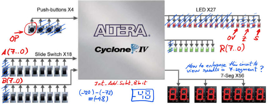
You can use a typical board DE2-115 populated with a target chip Cyclone IV FPGA EP4CE115F29C7 to try this demonstration circuit Int_add_subt_8bit. Use training boards and perform laboratory measurements to verify how the circuit being designed works for real.
|
|
Fig. 15. Example pin assignment for inputs and outputs. Board's switches are used for A(7..0) and B(7..0) operands. One push-button OP selects add or subtract operations. Eight green LED are used to represent signed integer results R(7..0), and three red LED are used for displaying flags. |
Assign pins with the pin planner spreadsheet.
Generate the output SOF file and run the Quartus Prime programmer to configure the chip. Lab 2 prototype shows you how to proceed.
Another complete prototype example is documented in the LAB4_2: designing an ALU_9bit.
| Home Term 26/27-Q1 Contact Products Electronic devices and companies Software Books Magazines Instruments DEE Library EETAC DEEL |

|
|
| Web activa des de 09/2001, @ F. J. Robert, Web editat amb Microsoft Expression Web 4. El contingut és un complement als materials d'estudi del curs Circuits i Sistemes Digitals disponibles al campus digital Atenea. Llicència:Reconeixement 4.0 Internacional de Creative Commons |