|
|
Bachelor's Degree in Telecommunications Systems and in Network Engineering |
|
Chapter 2 problems |
- D1.9 - |
A: 4-bit (nibble) shifter operator |
1. Specifications of the 4-bit shifter operator
In digital systems it is often necessary to have circuits that can shift the bits of a vector by one or more bit positions to the left or right.
Design a circuit that can shift a 4-bit vector W(3..0), also called nibble, one bit position to the right when a control signal SR = '1', and one bit position to the left when SL = '1'. When the control signals are not active SR = '0', SL = '0', the output is a copy of the vector W. We don't care about the output values if by any chance both control signals are activated SR = '1', SL = '1'; assuming that this condition will never occur. The symbol and operations of this device are represented in Fig. 1.
 |
Fig.1. Symbol of the Shifter_4bit. |
Complete the circuit's truth table sketched in Fig. 2 in a full A4 page .
 |
Fig.1. Truth table idea. |
Draw an example of timing diagram to be used later as stimulus in the VHDL testbench when verifying the synthesised circuit. Consider Min_Pulse = 2.45 ms.
The same project B3.9 is proposed in Chapter 3 for learning the basics of μC software organisation and basic digital I/O.
CPLD or FPGA target chip options:
Target option #1.: MAX II
Target option #2.: MAX 10 (*)
Target option #3.: Cyclone IV
(*) MAX10 chips are not used for running gate-level ModelSim simulation because Intel Quartus Prime does not generate the "*.sdo" file accompanying the "*.vho" translation of the technology view. Thus, you can run the timing analyser as usual, and change to another device family for performing examples of gate-level timing diagrams.
How many FPGA resources (logic cells, logic elements, etc.) are used? What is the percentage of the target chip used in this design?
2. Planning
Plan A structural circuit based on logic gates and equations in a single VHDL file. We have many strategies, for instance:
option #1: use Minilog to obtain PoS.
Project location:
C:\CSD\P2\Shifter_4bit_PoS\(files)
How many FPGA resources (logic cells, logic elements, etc.) are used? What is the percentage of the target chip used in this design?
option #2: use Minilog to obtain SoP.
Project location:
C:\CSD\P2\Shifter_4bit_SoP\(files)
How many FPGA resources (logic cells, logic elements, etc.) are used? What is the percentage of the target chip used in this design?
Plan B behavioural approach writing the truth table or the high-level description or algorithm in VHDL in a single file (flat).
Project location:
C:\CSD\P2\Shifter_4bit_B\(files)
How many FPGA resources (logic cells, logic elements, etc.) are used? What is the percentage of the target chip used in this design?
Chapter 2 problems |
- D1.9 - |
B: Barrel p-shifter n-bit operator |
1. Specifications of the n-bit barrel p-shifter operator
Let us propose the design of an n-bit configurable barrel shifter capable of shifting p-bit to the right or the left.
The idea is the following reference: Ercegovac, M., Lang, T., Moreno, J. H. Introduction to digital systems, John Wiley & Sons, 1999. Chapter 9, slides from 58 to 62.
 |
Fig.1. Symbol of the Barrel_p_shifter_nbit. |
For example, let us propose a 4-bit barrel 3-shifter (Barrel_3_shifter_4bit) capable of shifting in both directions. Discuss its symbol and truth table drawing all signals using positive indexes. Control Input P determines the number of bits to shift.
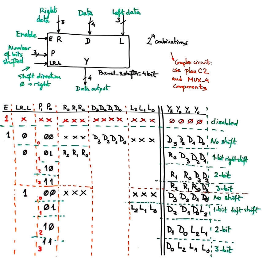 |
Fig.1. Symbol and truth table of the Barrel_3_shifter_4bit component adapted from the source. |
This is a large device and better to use plan C2 and MUX_4 components for designing it. The book reference gives an idea on how to start a first step considering only one shift direction.
After having studied P4 tutorials, additional questions can be added to our report. For instance:
-
Perform a gate-level simulation to measure propagation delays in a given signal transition.
-
Deduce the worst-case propagation delay running the timing analyser tool and calculate the circuit's maximum frequency of operation for the target chip used in the design.
| Home Term 26/27-Q1 Contact Products Electronic devices and companies Software Books Magazines Instruments DEE Library EETAC DEEL |

|
|
| Web activa des de 09/2001, @ F. J. Robert, Web editat amb Microsoft Expression Web 4. El contingut és un complement als materials d'estudi del curs Circuits i Sistemes Digitals disponibles al campus digital Atenea. Llicència:Reconeixement 4.0 Internacional de Creative Commons |