|
|
Bachelor's Degree in Telecommunications Systems and in Network Engineering |
|
|
|
Timer circuit. Phase #1: external CLK as time-base |
Dedicated processor: control unit + datapath
Design phases ==> #1: Timer ==> #2: Timer_LCD ==> #3: Timer_LCD_TMR0 ==> #4: Timer_LCD_TMR2
| 1. Specifications | Planning | Dev. & test | Prototype | report |
Design phase #1: Design a fixed timing period timer as shown in Fig. 1.
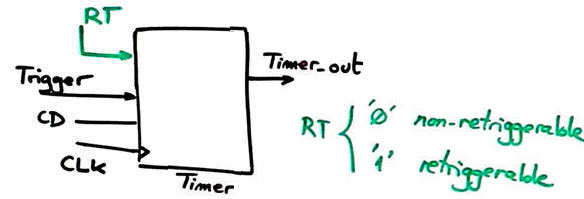 |
Fig. 1. Timer symbol. |
-
Timing period: TP = 18.5 s, as represented in Fig. 2.
-
A switch RT to select two modes of operation: retriggerable and non-retriggerable (consider planning two design steps).
-
External 50 Hz CLK (INT1) time-base. TB = 20 ms.
-
Trigger control signal push-button.
-
LED connected to Timer_out to visualise the timing period duration.
-
C language, coding in FSM style, dedicated processor approach.
-
Microcontroller PIC18F46K22.
-
MPLABX IDE + XC8 compiler + Proteus
-
CSD_PICstick board for prototyping experimentation.
-
VB8012 compact instrument for measurement and product characterisation.
We can easily imagine two design steps in this phase:
- Step #1. Basic non-retriggerable timer as for the the classic chip 74LS121. These are other similar classic timer circuits. Thus, we can draw the symbol in Fig. 1 without the RT input signal.
- Step #2. Retriggerable (RT = '1') and non-retriggerable (RT= '0') as for the classic chip 74LS122/123. This control signal RT is a switch to be polled (read or captured) connected to a given port pin, for example RA4.
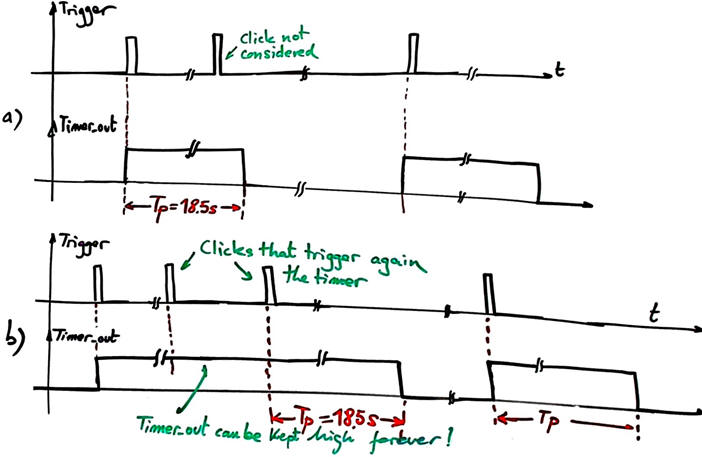 |
| Fig. 2. a) Waveform in non-retriggerable mode of operation. b) Retriggerable mode of operation where it is possible to keep Timer_out high forever if the user clicks Trigger repeatedly before the timing period ends. This particular circuit application has another widely used name: watchdog timer. |
| Specifications | 2. Planning | Dev. & test | Prototype | report |
As usual, we can conceive this circuit as if we were yet in P8 dealing with dedicated processors. Besides, the non-retriggerable timer was and solved as the version A at D2.21. Fig. 3 below shows a dedicated processor design for this timer. The FSM has to be able to attend trigger active edges to start operation and control the datapath, for instance a radix-2 up counter modulo 65536 (16-bit). In this way, for the TDP_CLK = 20 ms used as time base TB, we can generate a Timer_out signal that will last up to 21 min and 50 s.
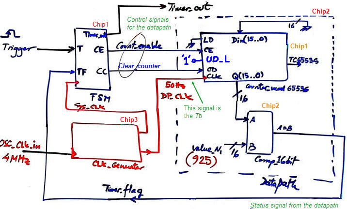 |
| Fig. 3. Example dedicated processor to perform the timer function as it could have been designed in Chapter 2 (L8.1). |
Study other materials, for instance these notes on how a programmable timer can be planned as in Chapter II using VHDL and FPGA/CPLD devices. Review as well the P8 highlighted programmable timer Timer_MMSS that is more complex but with a similar organisation.
Therefore, let us adapt such structures to a microcontroller.
A) Planning hardware
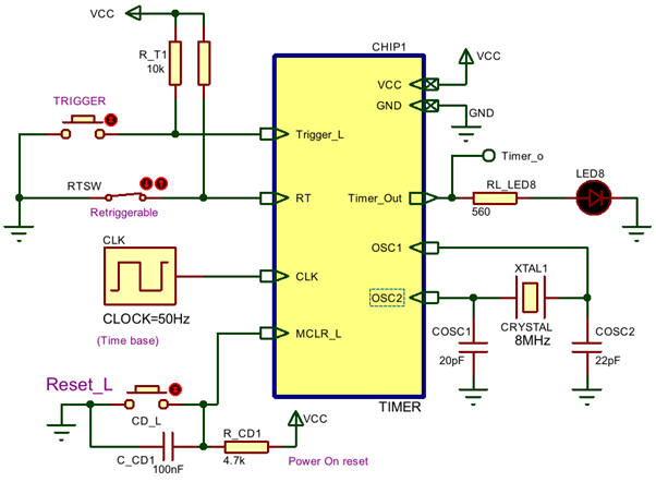
Determine where to connect the crystal oscillator (OSC), the master clear active-low or reset push-button (MCLR_L) control signals, RT, Trigger_L, time base CLK, and the output Timer_out.
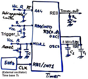 |
Fig. 4. Example of hardware connections. The interrupt-driven Trigger_L signal is a pushbutton connected at RB0/INT0. The interrupt-driven CLK external oscillator connected to RB1/INT1 is used to generate a time-base TB = 20 ms from which we will count "real-time". |
B) Planning software
Draw the hardware-software diagram imagining which mC resources may be connected to count real time.
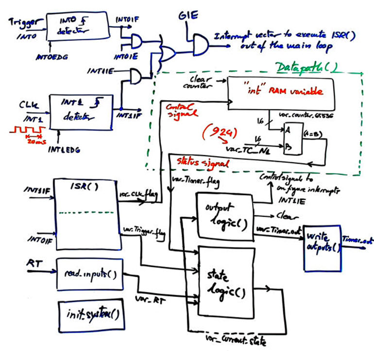 |
| Fig. 5. Hardware-software diagram. The interrupt service routine ISR() will generate two flag variables to run the FSM. |
List the RAM variables required and their type. Which variables will be flags as we name them attached to interrupts?
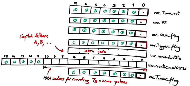 |
| Fig. 6. RAM variables. |
For instance, a good question to see the adaptability of this architecture: what would be the datapath structure if we like to count for a long timing period of TP = 2.5 h?
Draw the state diagram to run the FSM in control of the application. Be aware that the external CLK interrupt (var_CLK_flag) will be required (enabled) only when timing.
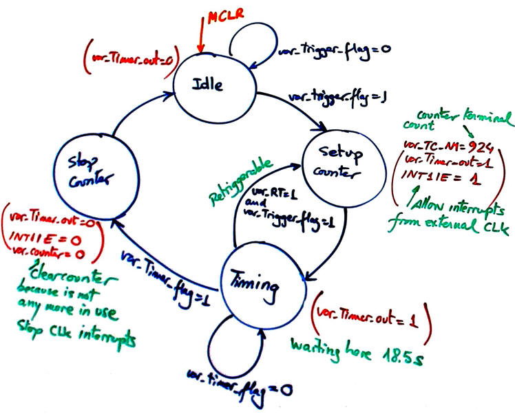 |
Fig. 7. Proposed state diagram for the FSM. The system is either Idle or Timing. However, peripherals and operational devices will require set up and stop extra states to configure them to work properly. Most of the mC peripheral devices may be kept disabled or even switched off for some µC models when they are not required. |
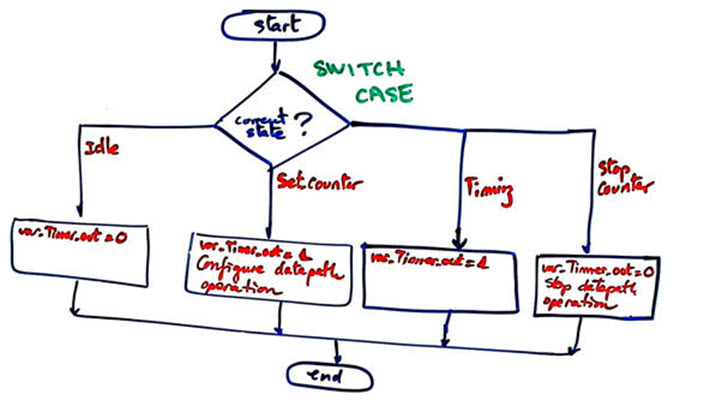
Fig. 8 shows our CSD flowchart to organise the software. The main loop will include the datapath() function running only when timing.
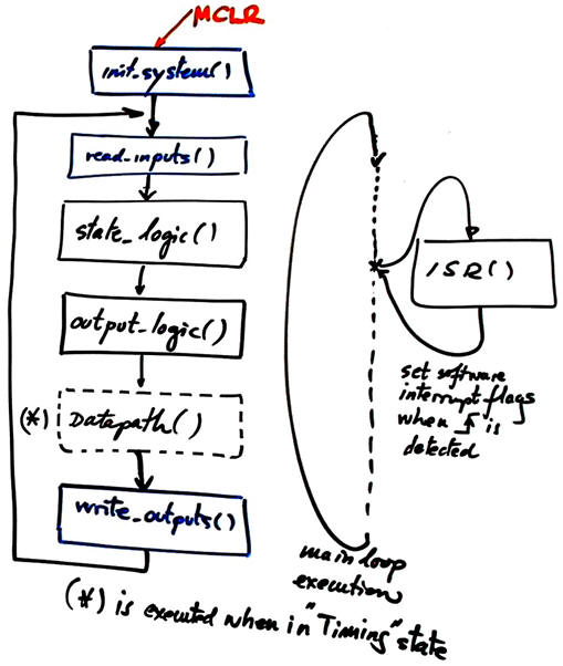 |
Fig. 8. General software organisation. ISR() will determine which is the interrupt source: trigger button (INT0) or external CLK (INT1). Datapath function for counting CLK periods will not be used when IDLE. |
Program init_system() function, configuring ports and interrupts INT0 and INT1.
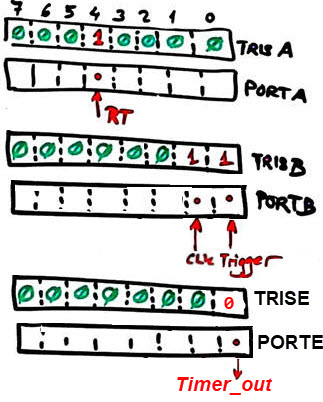 |
Fig. 9. These are the data direction registers
(TRIS) to configure the ports.
PORTB pin 0 is INT0, the Trigger_L push-button active-low to start timing PORTB pin 1 is INT1, the external oscillator CLK time-base TB. PORTA pin 4 is the the switch RT to select between the two modes of operation: retriggerable and non-retriggerable. PORTE pin 0 is the the output Timer_out. Unused port pins are configured by default as outputs. |
Program state_logic() so that all state transitions in Fig. 7 are implemented. Draw the truth tables and flowcharts as we usually do applying plan B.
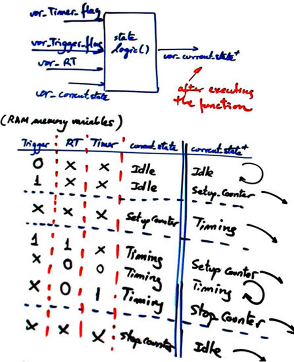 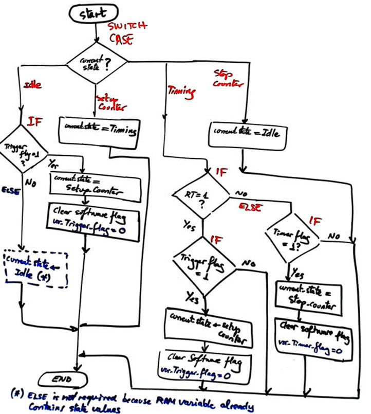 |
Fig. 10. State logic truth table and its equivalent behavioural flowchart from which C instructions are inferred directly without difficulties. |
Program output_logic(). Truth tables and flowcharts. As seen in Fig. 6 hardware-software diagram, output logic has to generate Timer_out circuit's output and control signals for managing the datapath counter.
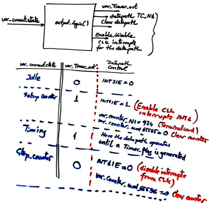  |
| Fig. 11. Output logic. Truth table and flowchart. |
Program datapath() as a P7 plan C2 counter the components of which are now solved in software.
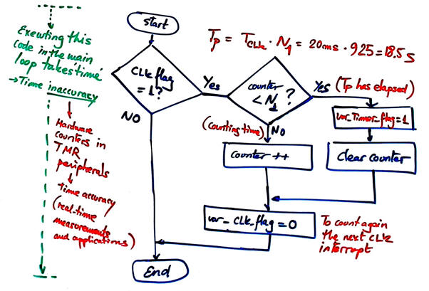 |
Fig. 12. Datapath is a counter described using RAM variables. Be aware that executing assembly instructions requires some μs, consequently introducing some systematic error if what we have in mind is measuring real-time. |
Write ISR() flowchart. so that the computer program can be sensitive to events such CLK rising edge and trigger button falling edges.
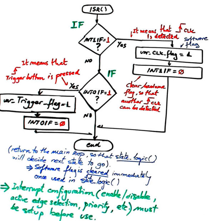 |
Fig. 13. ISR() flowchart. |
Program read_inputs(), write_outputs(). Truth tables and flowcharts.
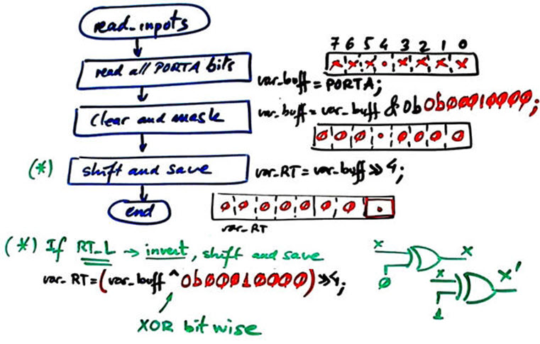 |
| Fig. 14. Read_inputs() captures RT value when executed. This value is saved in a convenient RAM variable var_RT. |
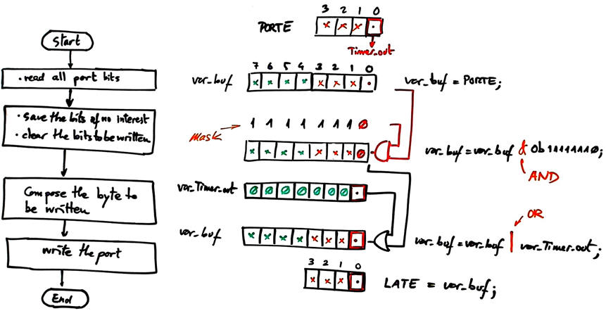 |
| Fig. 15. Write_outputs() copies var_Timer_out bit of interest to the port bit RE0. |
Target chip PIC18F46K22. Project location:
C:\CSD\P12\Timer\(files)
| Specifications | Planning | 3. Dev. & 4. test | Prototype | report |
A) Developing hardware
We capture the schematic in Proteus, as shown in Fig. 16. The "Timer.pdsprj" hardware file.
 |
|
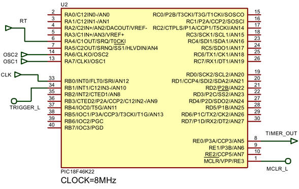 |
Fig. 16. Timer circuit captured in Proteus and the microcontroller connections to specific pins. |
B) Developing software
It is time to translate our plan flowcharts into C language. This source file example "Timer.c" containing the translation. Add the "config.h" header to your project.
Start a new project for the microcontroller's IDE MPLABX and its XC8 compiler. Let us select the target chip PIC18F46K22. In this way, we will produce the executable files:
(1) "*.cof" for running and debugging in Proteus
(2) "*.elf" for running and debugging using the MPLAB SNAP
(3) "*.hex" for programming the chip.
C) Step-by-step testing
The idea is, as usual, write and run a bit of code with both windows, the hardware Proteus environment and the software IDE running simultaneously for easy debugging. Use watch window and break points and also step mode to control the program sequence and execution and monitor RAM variables of interest for each function.
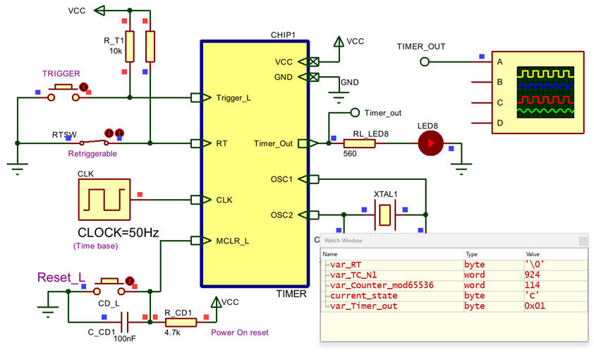 |
| Fig. 17. Basic timer running while watching RAM variables. |
Questions:
-
Use breakpoints to measure with precision the timing period TP.
-
Modify timing period to TP = 3.25 s. In this application the key point is the timing period precision. Is it 3.244 s or 3.246 s?
-
What can be done to improve the time resolution to 100 ms? Is it even possible to reach such low value?
| Specifications | Planning | Dev. & Test | 5. Prototype | Report |
Board CSD_PICstick . Target microcontroller: PIC18F46K22. Tools: MPLAB X + XC8 + Proteus + VB8012 compact instrumentation.
-
Measure the circuit timing period TP using the VB8012 logic analyser?
-
How to visualise the internal datapath var_Counter_mod65536 variable using MPLAB SNAP in-circuit debugger and also using the VB8012 logic analyser?
| Specifications | Planning | Dev. & Test | Prototype | 6. Report |
Follow this rubric for writing reports.
| Home Term 26/27-Q1 Contact Products Electronic devices and companies Software Books Magazines Instruments DEE Library EETAC DEEL |

|
|
| Web activa des de 09/2001, @ F. J. Robert, Web editat amb Microsoft Expression Web 4. El contingut és un complement als materials d'estudi del curs Circuits i Sistemes Digitals disponibles al campus digital Atenea. Llicència:Reconeixement 4.0 Internacional de Creative Commons |