|
|
Bachelor's Degree in Telecommunications Systems and in Network Engineering |
|
|
|
Timer circuit. Phase #3: TMR0 as time base |
TMR0 peripheral application as timer
Design phases ==> #1: Timer ==> #2: Timer_LCD ==> #3: Timer_LCD_TMR0 ==> #4: Timer_LCD_TMR2
| 1. Specifications | Planning | Dev. & test | Prototype | report | Annex |
Design phase #3: Design a fixed-time timer (for instance TP = 18.5 s) as represented in Fig. 1 replacing the internal RAM variable acting as a datapath counter by the TMR0 running as a time base TB = 4·TOSC = 500 ns. Let us consider the FOSC = 8 MHz crystal oscillator running the PIC18F46K22 µC on the CSD_PICstick board.
 |
|
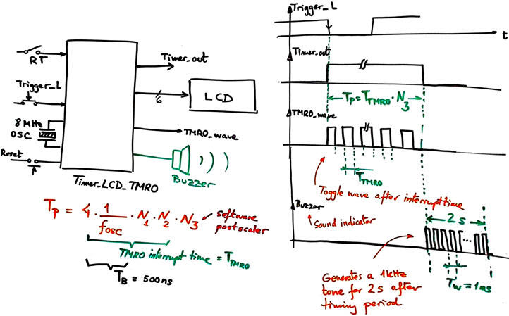
| Fig. 1. Project entity is the same in phase #2 eliminating the external CLK and replacing it by the internal TMR0. The quartz crystal that is used for running the µC will also determine time accuracy for this application. |
|
Common features:
- The same inherited features from project phase #1 Timer and phase #2 Timer_LCD.
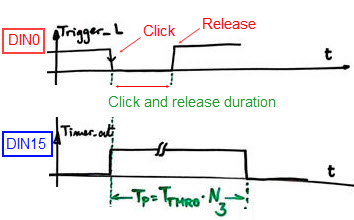
- TMR0 peripheral to generate from the TB = 500 ns a square output signal TMR0_wave with a period 2·TTMR0. (the waveform will toggle every TMR0 interrupt time).
- Optional: Add a buzzer that will sound for 2 s at 1 kHz tone once the timing period has ended.
Questions:
- Measure simulator's "real-time" using break points and step mode.
- Watch variables of interest.
- Modify parameters to generate TP = 2.23 s.
- Modify parameters to generate TP = 5.00 s when XTAL OSC is 12 MHz.
- Implement the circuit in the CSD_PICstick as a prototype and perform measurements to characterise the circuit's performance.
| Specifications | 2. Planning | Dev. & test | Prototype | report | Annex |
A) Planning hardware
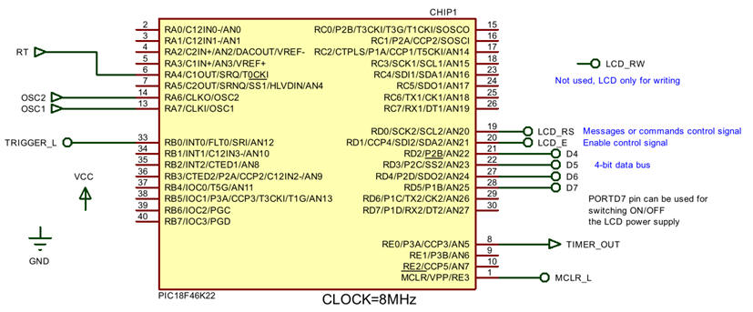
The schematic is simpler from phase #2 because CLK is removed. However, the TMR0 peripheral hardware is included in the project and it has to be configured correctly as our datapath for counting time. As shown in Fig. 2, we can use port pins connected to the CSD_PICstick available resources.
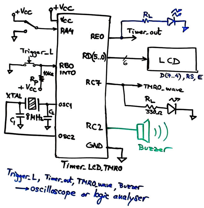 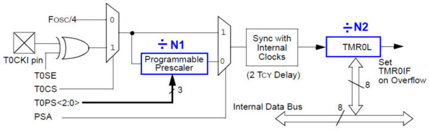 |
Fig. 2. Hardware schematic for the top timer application and also the TMR0 peripheral hardware to configure. |
B) Planning software
Study how the TMR0 works. Hardware configuration bits and registers: CLK edge, CLK source, prescaler selection, TMR0 in 8-bit or 16 bit mode, hardware interrupt on overflow (terminal count) TMR0IF and RAM variable var_TMR0_flag.
The datapath capable of counting real-time is the TMR0 peripheral configured as a timer; the control unit is a FSM running in the main loop. Draw the hardware-software diagram as in Fig. 3 and discuss it.
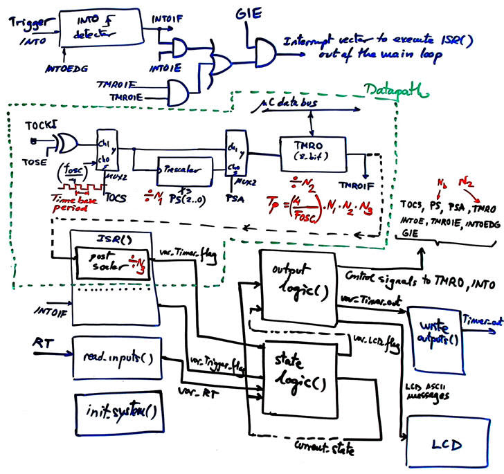 |
Fig. 3. Hardware-software diagram representing in dotted green lines the circuit that has become the datapath for calculating real-time from an internal time-base derived from system OSC. |
Explain the diagram of the TMR0 timer.
Design equation using the prescaler (N1), counter TMR0 (N2), and (software) postscaler (N3) when required:
TP = TB · N1 · N2 · N3 = TTMR0·N3
How to increase counting capacity to any arbitrary large timing period?
Fig. 4 shows how the state diagram may be adapted to generate timing periods using TMR0.
 |
Fig. 4. State diagram for the FSM. |
Program init_system() function configuring ports, interrupts and the TMR0.
 |
Fig. 5. TRIS registers. |
Discuss the state-logic() truth table and flowchart.
|
Fig. 6. state_logic(). |
Discuss the output-logic() truth table and flowchart.
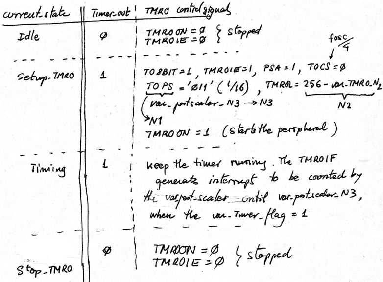 |
Fig. 7. Truth table for the output_logic() representing the instructions to the datapath and outputs. (update picture) |
Program ISR() to acknowledge interrupts from TMR0 and INT0 solving as well the datapath operation of real-time counting.
|
Fig. 8. ISR().(update picture) |
Program read_inputs(), write_outputs() as in phase #2 or phase #1.
Project location:
C:\CSD\P12\Timer_LCD_TMR0\(files)
| Specifications | Planning | 3. Dev. & 4. test | Prototype | report | Annex |
A) Developing hardware
This is the "Timer_LCD_TMR0.pdsprj" hardware including the LCD and the TMR0.
 |
| Fig. 8. The variable var_Timer_flag is derived from the internal TMR0. Therefore, the external pin RB1/INT1 is freed and can be used for another purpose. |
B) Developing software
These LCD library files "lcd.c", "lcd.h" have to be included in the project. The file "config.h" contains all the microcontroller configuration bits. This is the example software source code "Timer_LCD_TMR0.c". Generate the executable (*.hex) and debugging file (*.cof) for Proteus simulations.
C) Step-by-step testing
The idea is, as usual, write and run a bit of code with both windows, the hardware Proteus environment and the software MPLABX IDE running simultaneously for easy debugging. Use the watch window and break points to control the program sequence and monitor RAM variables of interest for each function.
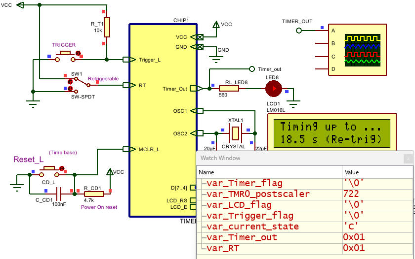 |
| Fig. 9. Circuit running and watching variables of interest. |
We can measure with the Proteus oscilloscope the circuit performance, for instance N3 = 125 generates a TP = 0.5 s, as shown in Fig. 10.
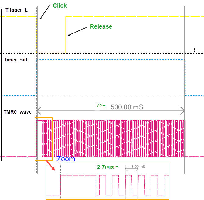 |
| Fig. 10. Waveforms printed from the Proteus oscilloscope. Once the trigger interrupt is generated, we can observe, zooming the TMR0_wave, how TMR0IF is asserted every TTMR0 = 4 ms. |
| Specifications | Planning | Dev. & Test | 5. Prototype | Report | Annex |
Board CSD_PICstick . Target microcontroller: PIC18F46K22. Tools: MPLAB X + XC8 + Proteus + VB8012 compact instrumentation.
Experiment #1: Run the application and visualise results using the board resources. This is for checking the installation of the tools and programming environment.
You will repeat the procedure described in the last LAB10.
Experiment #2 (optional): Download and program the target chip (*.elf) to use the in-circuit debugger. Watch RAM variables in MPLABX IDE. Add breakpoints and follow the program execution as we did in Proteus simulations.
Experiment #3: Visualise digital signals using instruments.
Fig, 13 shows the connections to the VB8012 using the 40-pin header.
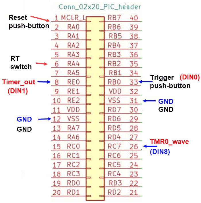 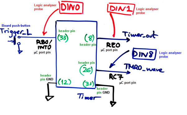 |
Fig. 13. Attention: Draw this schematic in a sheet of paper before prototyping and be aware of the port pins, power supply, inputs and outputs used, and the instrument probes. 40-pin header connections to the protoboard and the VB8012. And yet another schematic symbol indicating signals of interest, header pin numbers and instrument probes in different colours. When experimenting in the laboratory, it is crucial to put all your senses in the circuit to avoid short-circuits and other costly hazards. |
In a first step, as sketched in Fig. 14, we connect GND, VCC and the duplicated LED at Timer_out.
 |
Fig. 14. Draw this sketch in paper. Protoboard short connections to power rails and duplicate the Timer_out LED. We use a an electrolytic capacitor as a buffer for energy storage; be aware of its polarity. |
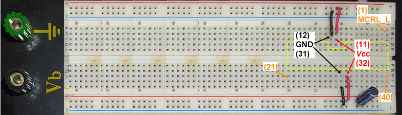 |
Fig. 15. Picture on how the circuit looks like before adding the duplicated Timer_out LED. |
Attach the 40-pin cable adaptor as shown in Fig. 16. Power on the CSD_PICstick to run again the experiment #1. Check that the circuit works and the LED lights for the programmed TP.
 |
Fig. 16. Plugging the 40-pin flat cable adaptor. The Timer_out signal is replicated from the expansion connector pin 8 (RE0) to a red LED. |
In a second step, as sketched again in Fig. 17 and visualised in Fig. 18, we add the LCD contrast potentiometer V0. We also connect the LCD backlight LED to A = +Vcc and K = GND.
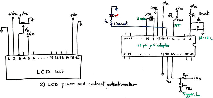 |
Fig. 17. Draw this sketch in paper. It shows how to power the LCD kit. |
 |
Fig. 18. Picture on how the LCD is powered. |
Now we have to verify that these simple connections are right and the breadboard is correctly powered. When experimenting in the laboratory, it is crucial to put all your senses in the circuit to avoid short-circuits and other costly hazards. Attach the 40-pin flat cable adapter and plug the LCD male header to the indicated location.
NOTE: To avoid hazards, be sure that the CSD_PICstick board is unplugged every time you add new connections or wires to the protoboard.
 |
Fig. 19. Running the experiment #1 with the expansion connector plugged to the breadboard. We also insert the LCD to check whether it is correctly powered. Its backlight is turned on. Use a screwdriver to adjust the LCD contrast by means of RV2, the 10 kΩ potentiometer. |
When this second step works correctly, switch off the CSD_PICstick DC power adapter and unplug the cable adapter and the LCD to continue.
In a third step, as shown in Fig. 20, we use 20 cm male-male flexible wires for facilitating the connections to the 6-wire LCD parallel interface bus.
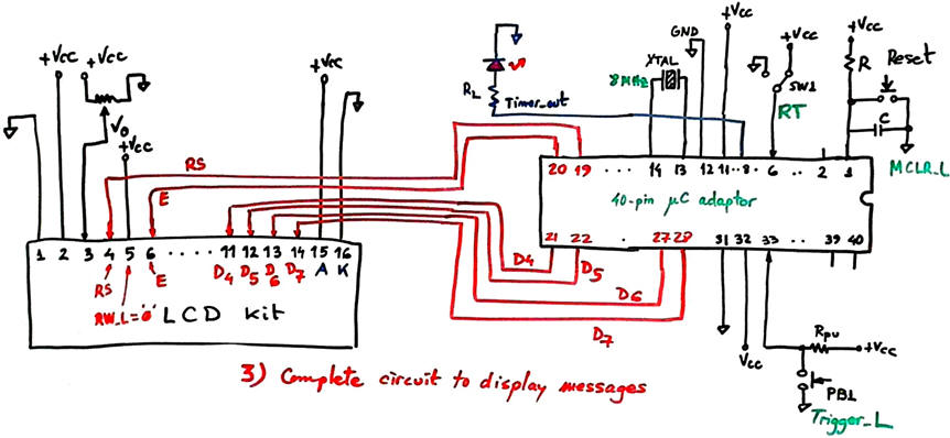 |
Fig. 20. Adding the 6 male-male wires to interface the LCD kit to the 40-pin adaptor. |
Now we have to verify that these new connections are right. This is the complete experiment to represent ASCII messages on the screen. Attach the 40-pin flat cable adapter and plug the LCD male header to the indicated location. Power on the CSD_PICstick. The LCD will display messages and clicking Trigger_L will generate the configured timing periods TP.
In the next fourth step we will monitor signals using the VB8012 compact instrument. We connect the long male header pins for the logic analyser probes DIN0 - Trigger_L, DIN15 - Timer_out, DIN16 - TMR0_wave.
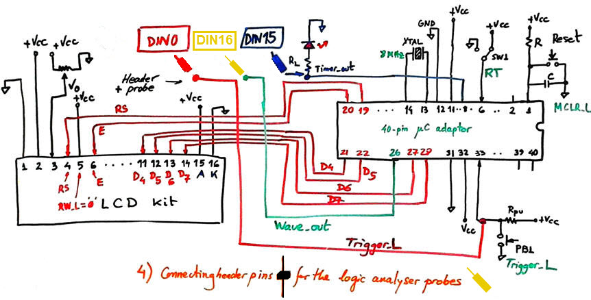 |
Fig. 21. Adding header pins for the logic analyser probes. |
The next photography Fig. 22 shows the completer prototype layout.
 |
Fig. 22. Flexible wires for interfacing the LCD and the instrument probes by means of long male header pins. |
Attach the 40-pin flat cable adapter and plug the LCD male header to the indicated location. Power on the CSD_PICstick to run again the experiment as shown in Fig. 23. The LCD will display messages and clicking Trigger_L will generate the configured timing periods TP.
 |
Fig. 23. The complete experiment running in the protoboard and prepared for connecting the logic analyser. |
In a fifth step, as shown in Fig. 24, run the WaveForms app and open the logic analyser instrument.
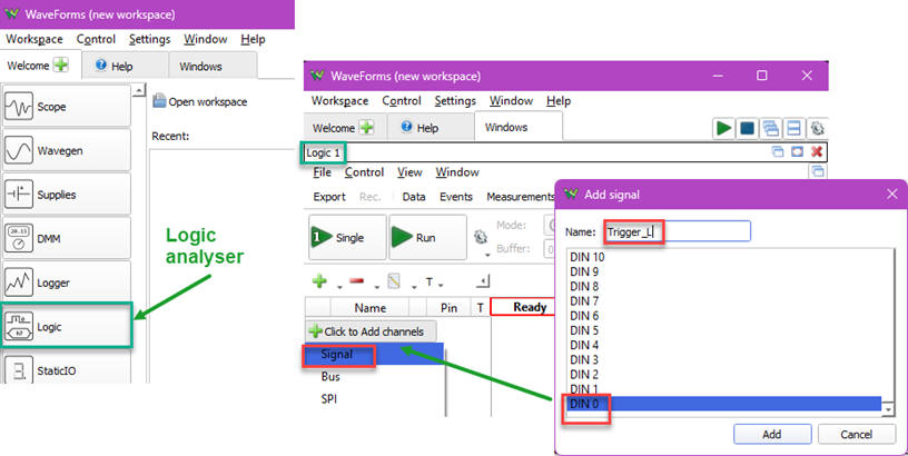  |
Fig. 24. The final circuit for measuring signals with the VB8012 and experimenting. |
We have to attach the instrument probes. Do it as follows: one signal at a time discussing what the instrument is measuring:
1) Connect DIN0 - Trigger_L. Run the logic analyser triggering DIN0 on falling edge. Observe the full event of clicking and releasing the PB1.
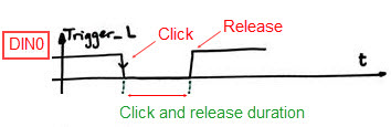
For instance: use cursors to measure your click duration. Use a time base around 100 ms/div. Click and measure several times.
2) Connect DIN15 - Timer_out. Add a new signal to the logic analyser and observe the timing TP event.
For instance: use cursors to measure TP. Program the µC with different values (output_logic(), setup_counter state).
3) Finally, connect DIN16 - TMR0_wave to observer how the TMR0IF generates the TTMR0 = 4 ms = TB · N1 ·N2.
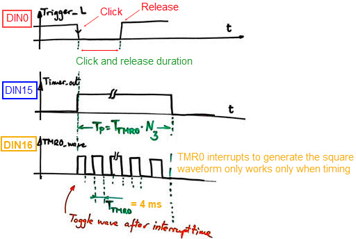
For instance: measure TTMR0. Change N1, N2 to program TMR0 overflows every TTMR0 = 6 ms.
Experiment with the full circuit, capture the waveforms and measure the circuit parameters. Save your instrument VB8012 setup: "VB8012_setup_Timer_LCD_TMR0.dwf3work" in case you like to continue another time.
Capture and comment screens of interest for your reports as shown in Fig. 25.
 |
Fig. 25. Printing and annotating the captured logic analyser waveforms. In this example, it is displayed a timing period TP = 0.5 s (N3 = 125). |
Similar measurements for TP = 1.32 s (N3 = 330).
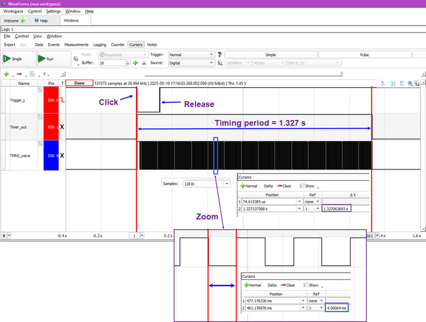 |
Fig. 26. Printing and annotating the captured logic analyser waveforms. We can also zoom into a particular time slot for measuring correctly the half period of the Wave_out signal TTMR0 = 4 ms. |
How to measure the timing period TP precision? For instance, is it possible for TP = 500 ms to reach a precision of ±5µs?
Once the experiment completed, it is time to look further into details using the MPLAB SNAP in-circuit debugger (experiment #2).
It is also time to enhance the product features. For instance, study how to modify the system to add a buzzer to sound an alarm with a 1 kHz tone for 2 s when the timing period has finished.
If more precision is required, TMR2 can be used instead of TMR0 as proposed in this design phase #4: Timer_LCD_TMR2.
| Specifications | Planning | Dev. & Test | Prototype | 6. Report | Annex |
Follow this rubric for writing reports.
Annex: Example on how to print dynamic data on the LCD |
Specifications
We can enhance the software to represent the count down on the LCD as dynamic data, as it is typical for commercial timers. For instance, let's visualise a time resolution of a tenth of a second while counting down.
Planning
This processing is solved in Timing state (Fig. A1). To solve this problem, we consider to print on the display a new variable var_Count_down = var_TP - var_Current_time calculated every 0.1 s (0.1 s = 25 * TTMR0).
Overflow hardware interrupts from TMR0 occur every TTMR0 = 4 ms, therefore, we need to count 25 interrupts to set the var_LCD_flag to refresh the screen with the updated value var_Count_down.
 |
| Fig. A1. Displaying "real-time" in one-tenth of a second resolution on the LCD. |
Project location:
C:\CSD\P12\Timer_LCD_TMR0_Dyn\(files)
Development and testing
The modified Timer_LCD_TMR0.c solved using float type variables.
 |
Fig. A2. Picture of the timer representing and updating time every tenth of a second. |
Note: When dragging and dropping floating point variables to the watch window they appear as "unspecified".
 |
Fig. A3. |
You can solve this problem in this way:
1) Edit the PIC18F46K22 component properties as a text to add this new property: {{DT_FLOAT=MICROCHIP_BIGENDIAN}
 |
Fig. A4. |
2) When running in step by step mode, select the variable and change its type to IEEE Double (8 bytes):
 |
Fig. A5. |
And, select another time and tick "Big Endian"
 |
Fig. A6. |
In this way, when running you have to be able to monitor the floating point values correctly:
 |
Fig. A7. |
Discussion and measurements:
- Compare the memory occupation when using LCD and sprintf functions. (a) printing only static data. (b) printing dynamic data. Why such large increase on RAM and ROM space?
a)
b)
- The implementation is based on floating point operations using seconds as units TB = 1e-7 s). How to do it using long int type (uint32_tem>) and µs as time base (TB = 0.5 µs · N1 = 16 µs).
- Measure the timing period precision. Is is better or worse that the circuit representing only static data on the display? How long does it take to refresh the dynamic data on the screen every 100 ms?
- Visualise the waveforms, monitor TMR0_wave. Is is a good idea to use the LCD for printing fast dynamic data? Which may be an efficient alternative?
| Home Term 26/27-Q1 Contact Products Electronic devices and companies Software Books Magazines Instruments DEE Library EETAC DEEL |

|
|
| Web activa des de 09/2001, @ F. J. Robert, Web editat amb Microsoft Expression Web 4. El contingut és un complement als materials d'estudi del curs Circuits i Sistemes Digitals disponibles al campus digital Atenea. Llicència:Reconeixement 4.0 Internacional de Creative Commons |