|
|
Bachelor's Degree in Telecommunications Systems and in Network Engineering |
|
Chapter 2 problems |
- D2.21 - |
Programmable timer (version A) |
1. Specifications
Conceive a real-time timer to count CLK pulses as represented in Fig. 1. The timing period will be TP = M·TCLK where the M parameter can be adjusted to any positive number. After detecting the trigger (TRG) positive edge, the timer out (T_Out) signal is kept high for a duration TP.
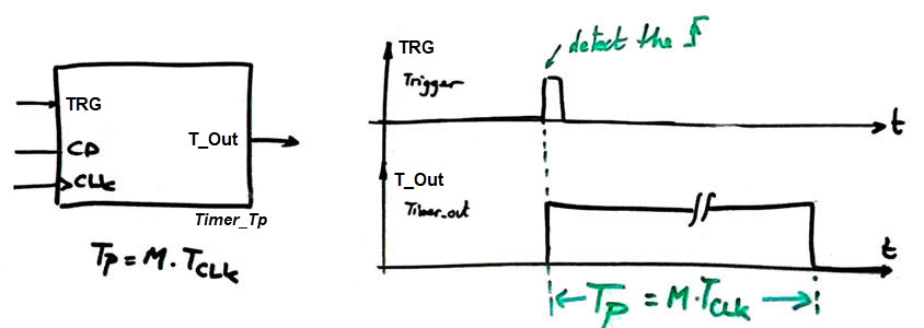 |
Fig. 1. Initial idea of a configurable timer. |
For example, we can generate a Timer_12_5s circuit with a timing period of 12.5 s using a CLK frequency of 12 kHz, and adjusting M = 150000.
More ideas in this timers unit and also in this LAB11.
2. Planning
Let us use a simple dedicated processor architecture, a FSM controlling a configurable binary counter.
 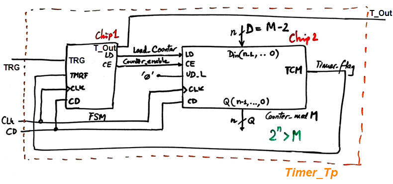 |
Fig. 2. The timer conceived as a simple dedicated processor. The datapath circuit is a configurable counter. |
Three states are required to operate this basic timer, as shown in Fig. 3.
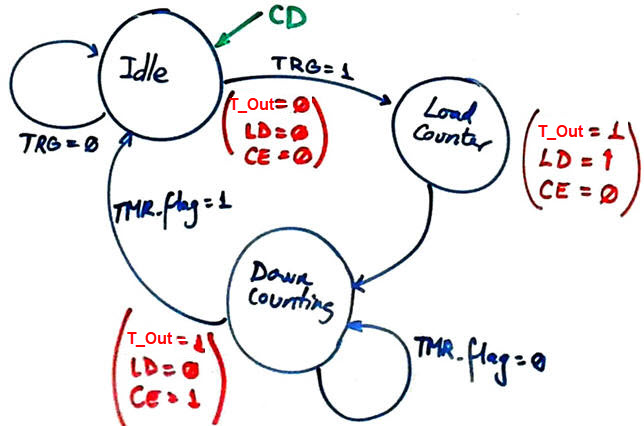 |
Fig. 3. State diagram. |
The timing diagram can be inspected in Fig. 4. Complete it with the datapath control signals and also include the internal signals current_state and next_state from the FSM.
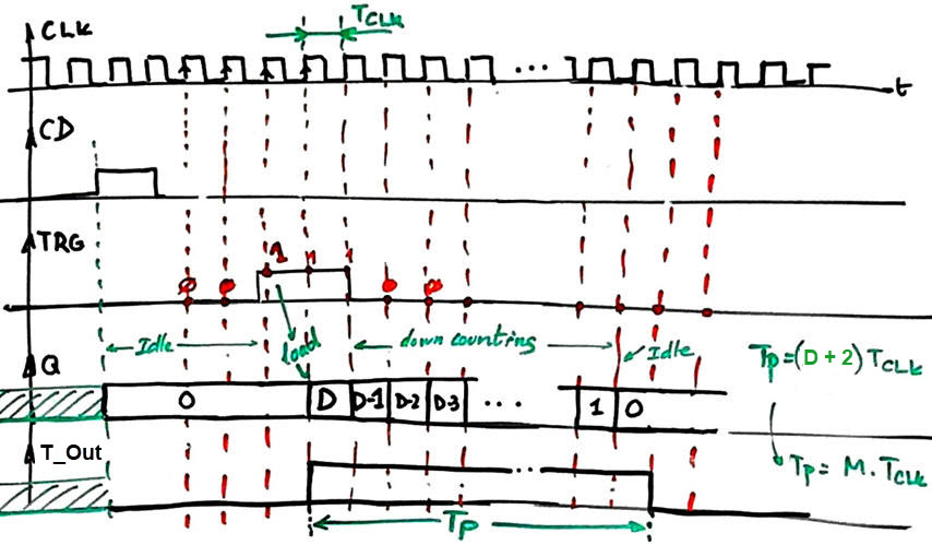 |
Fig. 4. Example timing diagram that later can be reproduced using ModelSim functional simulations. We can load the counter with a number D = M-1 (one CLK cycle is used for loading the counter Chip2 ). |
Fig. 5. Adapting the FSM to this project. |
Fig. 6. State register using D_FF and state encoding in one-hot. |
Fig. 7. CC1 truth table and its flowchart representation using plan B. |
Fig. 8. CC2 truth table and its flowchart representation using plan B. |
Let us select a Cyclone IV FPGA and this project location:
C:\CSD\P8\Timer_Tp\(files)
3. Development
This is the Chip1 translation "FSM.vhd" using our recipe in plan C1.
Let us fix M = 1024. This is the Chip2 translation "Counter_mod1024.vhd". It is inferred using plan Y adapting the standard Counter_mod16.
This is the top "Timer_Tp.vhd" using plan C2.
Fig. 9. RTL view. |
Fig. 10. Technology view implemented in a Cyclone IV FPGA. |
4. Test (functional)
The required testbench fixture is sketched in Fig. 11.
Fig. 11. Testbench schematic. |
And therefore, we can translate it as usual in two steps (template + signal stimulus) as "Timer_Tp_tb.vhd".
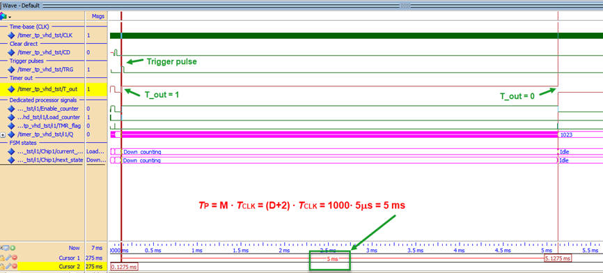 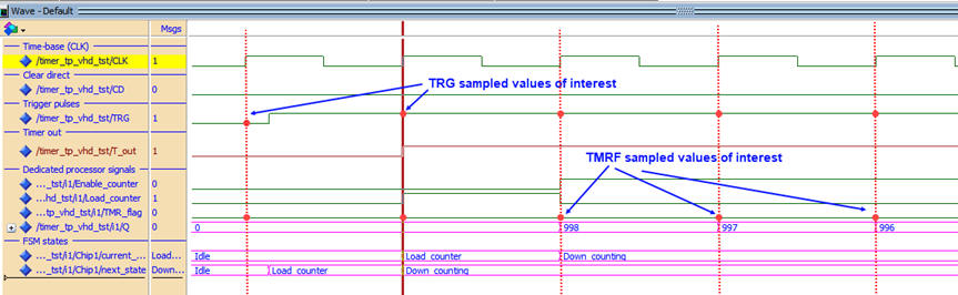 |
Fig. 12. Ideal results from ModelSim functional simulations. In this waveform we fix the following parameters: M = 1000 and fCLK = 200 kHz. We can zoom near the trigger pulse to watch how states evolve in time. We can also pay attention on the sampled values of interest (external TRG signal and datapath status signal TMR_flag). This is the instrument setup "wave.do". |
5. Test (gate-level)
We can determine the propagation time from CLK to output tCO and thus the maximum CLK frequency. Which is the minimum TP that can be configured?
Fig. 13. Gate-level measurements for a Cyclone IV device. |
Fig. 14. Timing analyser |
If you like to time a month (Timer_1month), how many resources and D_FF are used in a platform DE10-Lite?
Chapter 2 problems |
- D2.21 - |
Programmable timer (version B) |
1. Specifications
(under revision)
Design a programmable timer using the dedicated processor strategy containing datapath circuits for performing timing operations and control unit ( FSM) to sequence the process.
The same project designed programming a μC is in D3.21.
 |
Fig 1. Programmable timer symbol (Visio) and a sketch on how it has to work. The number T is T1 or T2 or T3 or T4 depending on the Sel_time input. Therefore, counting time means counting pulses or TCLK periods (the time base) which have a vey well known and stable frequency. Generally, this TCLK signal is derived from quartz crystal using CLK generator circuits. The system runs synchronised to CLK. |
 |
|
- 8-bit data to program the timing period.
- Four programmable timing periods: T1, T2, T3 and T4.
- Trigger signal to start the timing period. Non-retriggerable device.
- Timer_out signal goes high while timing.
- Timer_flag signal goes high to indicate the end of the timing period, thus allowing expandability connecting this signal to the Trigger input of the next device.
- Dedicated processor design strategy.
2. Planning
Some ideas and files to start the project:
These are the initial ideas and in Fig. 2 there is the general architecture of a dedicated processor that we'll adapt to this problem. External inputs and status signals from the datapath establish the next state to go.
|
|
Fig. 2. General architecture of a dedicated processor where the control unit or controller is a FSM that handles the circuits in the datapath which are in charge of processing information. |
- Draw the state diagram of the Timer_FSM.vhd and infer the number of registers required in this project.
- Solve the Timer_FSM.vhd component:
- Adjust the general FSM topology to this problem. To which block (CC1, CC2, state register) is connected every input and output?. How many r bits are required for coding the current and next state signals [r = number of states if one-hot; r = (1/log 2)·log (number of states) if binary or Gray]
- Deduce the truth table of the CC1 and CC2 and their corresponding flow charts.
- Write the VHDL code of the finite state machine adapting an example from our web.
- Develop the Octuple_MUX4.vhd required to select the time period.
- Develop the 8-bit down counter with parallel input. Counter_8bit.vhd
- Develop the data registers. Data_register_8bit.vhd
- Optional component: Exact timing using an arithmetic circuit to offset the FSM overhead bits (adder or substractor from P4).
- Connect all the components (Counter_8bit.vhd, Octuple_MUX4.vhd, Adder_8bit.vhd, Data_register_8bit.vhd) together in the top Programmable_timer.vhd, file and implement and test the system using the Programmable_timer.vht.
- Some files to start this plan C2 project. Adder_8bit was studied in Lab3. The top schematic is given, but some components with their empty architectures are yet to be designed. Thus, the point is that all the files included in the project can now be compiled together and the EDA tool generates the top level RTL schematic represented in Fig 3.
 |
| Fig. 3. The top RTL view where all the components are
connected. |
NOTE: the synthesiser shows you this error because some components are not finished.

 |
| Fig. 4. The internal datapath structure. |
 |
| Fig. 5. The timer FSM that controls the sequence of operations to be solved by the datapath. |
- Run the EDA tool to synthesise the circuit and print and comment the RTL schematic.
- Check the number of registers (D_FF) used in the target chip and justify the value. Does it match with your initial value?
- Start the test bench template and add the CLK and inputs activity translating the timing diagram. Make all the timing relative to the CLK_Period constant.
- Complete the template testbench file named Programmable_timer.vht translating a timing diagram like the one represented above in the specifications into CLK and input signals stimulus processes.
- Functional simulation. Run the EDA VHDL tool and demonstrate how the circuit works adding comments to the printed sheet of paper containing the waveforms. Your system may works like the timing diagram discussed in class.
- Run the gate-level simulation of the project and measure the maximum frequency of operation. It is worth to know exactly which is the maxim CLK frequency for a given target CPLD or FPGA chip.
Chapter 2 problems |
- D2.21 - |
Programmable timer (version C) |
1. Specifications
(under revision)
Let us interface the Programmable_timer developed above and the registered 16-key matrix encoder in D2.15 to generate a keypad-controlled programmable timer.
 |
Fig 1. Symbol and electrical schematic for the proposed keypad-controlled programmable timer. |
- Solve the CLK generator chip to generate 100 kHz (SCLK), 200 Hz (MCLK) and the time base signal of 1 Hz from the crystal quartz oscillator available in the training board. For instance, 25.175 MHz in Altera's UP2, 50 MHz in Digilent NESYS 2 board or 1 MHz CLK signal in HWD-LC4128V from Lattice Semiconductor.
- Organise the system architecture to read T1 time from the keypad (maximum time is 99 s) and trigger the timer when clicking the key '*' (or 'F') . Key 'C' is the system reset (CD).
Optional features:
- The ready green LED can be set in intermittent mode at 2 Hz rate when timing.
- When the timing period ends, generate a 10 s audible sound (square wave of about 1.5 kHz).
- Etc., for example, replace this local keypad by a computer connected using a RS232 USART or a I2C bus to the programmable timer.
2. Planning
Some ideas and files to start the project:
Organise the hierarchical architecture represented in Fig. 2.
 |
Fig. 2. Schematic (click to zoom). Discuss what section of the circuit is the datapath, and which wires are: status signals, control inputs, control outputs data inputs and data outputs. |
- Chip 6. Plan the CLK_generator.vhd. Explain how it works and the signals generated, adapting it to your board.
- Chip 4. Design the combinational circuit BCD_BIN_converter_2dig (symbol) used for translating the BCD keypad codes to a binary number, thus it can be understood by the programmable timer. In this application the maximum value that can be programmed is 99 s corresponding to the 7-bit radix-2 number "1100011".
Let us show you the power of VHDL synthesising algorithms in hardware. These are two proposed plans.
- Plan A is structural as it was learnt in P3.
- Plan B is behavioural schematic. Write the code VHDL, inspect the RTL, the technology and test it functionally or at the gate-level using for example this test bench.
 |
Fig. 4. RTL view of the plan B converter's equation. |
- Chip 1. Matrix_encoder_16key_registered from D2.15.
- Find VHDL code for the data registers.
- Discuss the state diagram for the Chip7 Control_FSM.
- Mount the top circuit assembling all the components into a single project.
- While examining the RTL schematic, be aware of the number of registers (D_FF) used in the target chip and justify the value. Does it match with your initial estimation?
Chapter 2 problems |
- D2.21 - |
Programmable timer (version D) |
1. Specifications
(under revision)
The user enter a three digit number from a numerical keypad. Then clicks start (ST) to down counting from the number entered. While down counting a LED is blinking with 0.6 s period.
In a design phase #2 this feature can be considered: when zero is reached, a 1.2 kHz sound wave drives a buzzer for 5 s.
The same project designed programming a μC is in D3.13.
Some ideas to kick off the project:
Indeed, this application is a timer device based on a 3-digit BCD down-counter, and its structure and components will be similar to P8 highlighter project. We can imagine that this instrument, in its first design phase is counting in seconds, thus the maximum number is 999 s.
| Fig. 1. Initial sketch representing the symbols and the main signals. |
An idea of the waveforms from the circuit is represented in Fig. 2. We can imagine that in an initial state the machine is sampling the keypad: the digits are shifted from units to hundreds and last three captured digits represent the timing period in seconds.
 |
| Fig. 2. Example of initial timing diagram. The 1.2 kHz SW signal can be generated in a design phase #2. |
A way to start capturing digits is considering the hardware in Fig. 3. We have an Enc_10_4 whatever combinational (DT2.5, L2.3) or matrix (P6). When the user is clicking a key, GS = '1'. We can use this signal to control the sequence of states and be able to save in Data_Reg_4bit and shift left the digits inputted. We also may consider that at any time the user can click the start button ST to generate the timing period TP at Timer_out, the LED intermittency at Timer_LED and the sound waveform at SW.
 |
| Fig. 3. Example of datapath hardware sketch for saving and shifting left digits. In this case for capturing input information, the seconds count to time. The key concept is that LD = '1' only for one CLK period when the user is clicking. The digit chain can be expanded to the desired number of digits. |
 |
| Fig. 4. Convenient initial state diagram to capture digits when the key is clicked. It works a loop capturing and shifting left digits. It has to be continued to control the remaining circuits of the datapath when the user presses ST = '1'. |
Naturally, the complete datapath circuit will also include the Counter_BCD_3digit with parallel load (LD) and Din. It is sketched in Fig. 5. In this project, this Chip5 is the main component. Thus it is a good idea to design and test it as an individual project in an initial design step. We can invent it only for down-counting operations (no need of UD_L control signal).
- How to design the Counter_BCD_3digit chaining/expanding 1-digit BCD counters from this Counter_BCD_1digit plan Y tutorial adding the parallel load LD?
- Or, how to design it studying and adapting the Hour_counter P7 highlighted project based on Counter_mod16?
Only when Chip5 is fully tested and working correctly we can use it in this application.
 |
| Fig. 5. Example of internal design of the Datapath circuit, an operational unit that encodes, decodes, count, select and register the data from the keypad. The control unit (FSM) will order and organise the sequence of operations. The 5 s timer for controlling the sound wave can be included in a design phase #2. |
In this way, we can deduce and draw as shown in Fig. 6 a possible dedicated processor for solving the main tasks of this timer/down-counter.
 |
| Fig. 6. Example circuit for a dedicated processor. |
The control unit (FSM) can run an state diagram as shown in Fig. 7. The status signal Z_flag from the datapath indicates when the down count has reached zero (terminal count) to stop timing and trigger on the falling edge the 5 s timer that will enable the sound wave (TSW).
 |
| Fig. 7. Only once the hardware is invented we can imagine the required states to control and run this application. |
In a first version of the CLK_Generator you can generate only one CLK signal, for example CLK_200Hz_SQ to run both the FSM and the datapath. In this way you can check whether the operations of reading and saving digits, loading the counter and down counting work correctly.
Design phase #2: Include the 5 s timer that controls the sound waveform (SW) output.
Optional design phase #3: How to enhance the circuit to generate accurate pulses in nanoseconds (ns), microseconds (μs) and milliseconds (ms). The concepts of accuracy, precision, resolution and sensitivity in instrumentation.
| Home Term 26/27-Q1 Contact Products Electronic devices and companies Software Books Magazines Instruments DEE Library EETAC DEEL |

|
|
| Web activa des de 09/2001, @ F. J. Robert, Web editat amb Microsoft Expression Web 4. El contingut és un complement als materials d'estudi del curs Circuits i Sistemes Digitals disponibles al campus digital Atenea. Llicència:Reconeixement 4.0 Internacional de Creative Commons |