|
|
Bachelor's Degree in Telecommunications Systems and in Network Engineering |
|
|
|
ALU_9bit prototype for laboratory experimentation |
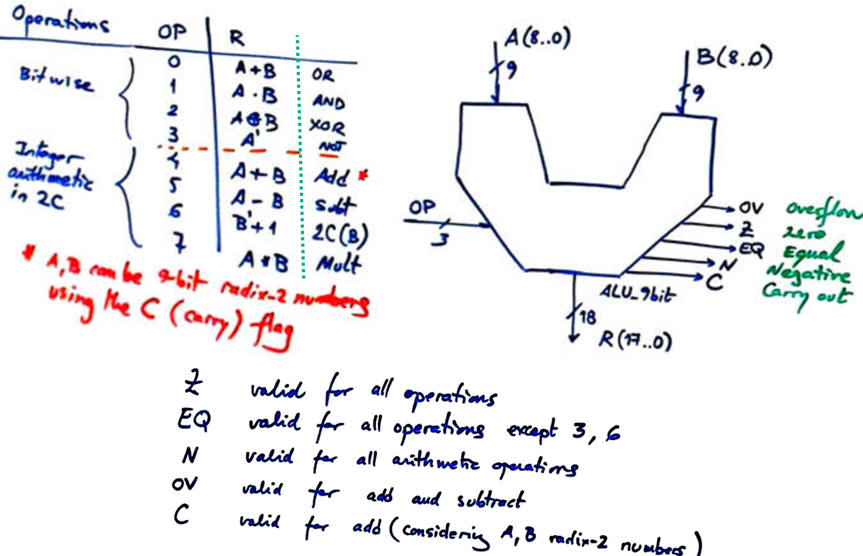
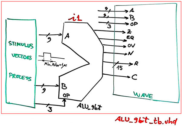
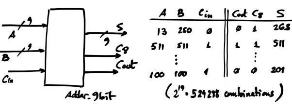
9-bit arithmetic and logic unit
| Prototype specifications | Planning | Development | Test & measurements | Lab |
Laboratory prototyping is the next phase in the circuit design flowchart (section #6). We have to advance from computer simulations to real hardware that can be industrialised in factories and sold as products.
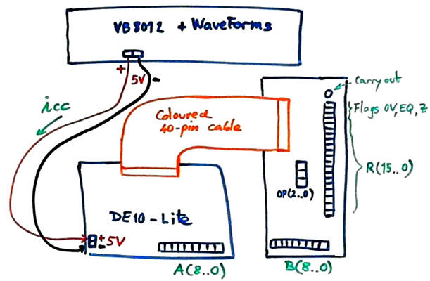
To practise with arithmetic and logic circuits, we conceive the arithmetic and logic unit (ALU) sketched in Fig. 1, an ALU_9bit capable of performing eight logic and arithmetic operations, in a DE10-Lite board populated with an Intel MAX10 FPGA chip. The entity has 21 inputs and 23 outputs.
 |
|
Fig. 1. ALU_9bit symbol and projected operations. |
Pre-lab activities #1:
Write a draft of the truth table considering arithmetic and logic operations and expected results. Deduce the operands and result ranges for arithmetic operations. Complete (at least) the 8 lines of the truth table using the given values A = "011111111" and B = "100000001". Do the arithmetic operations in binary 2C and check your results in decimal. Do the bitwise operations. Remember that these input values A and B are simple binary combinations when performing logic operations, and integer numbers in 2C when performing arithmetic operations: A = (011111111)2C = (+255); B = (100000001)2C = (-255). Draw a sketch of a timing diagram. Which can be the operation to take longer to process (longest propagation time)?
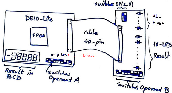
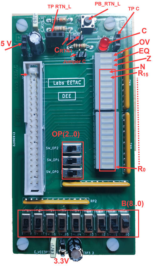
When thinking about the real implementation of such a circuit, the DE10-Lite board switches can be used for inputting operand A. The six 7-segment displays can be used for representing results as BCD numbers for arithmetic operations. In this way, we can populate a PCB connected through the 40-pin general-purpose input-output (GPIO) connector for capturing the operand B, selecting operations OP, representing the full binary result R(16..0) in an LED array and lighting the status flag indicators as well.
 |
|
Fig. 2a. DE10-Lite and PCB prototype for accommodating all inputs and outputs. The board contains many more resources that are not used in this laboratory experiment. |
Hence, the laboratory implementation of the ALU_9bit will require a top view including switches for operands and operations, 7-segment displays and LED for results and flags. We are using only a few resources from the DE10-Lite training board.
 |
|
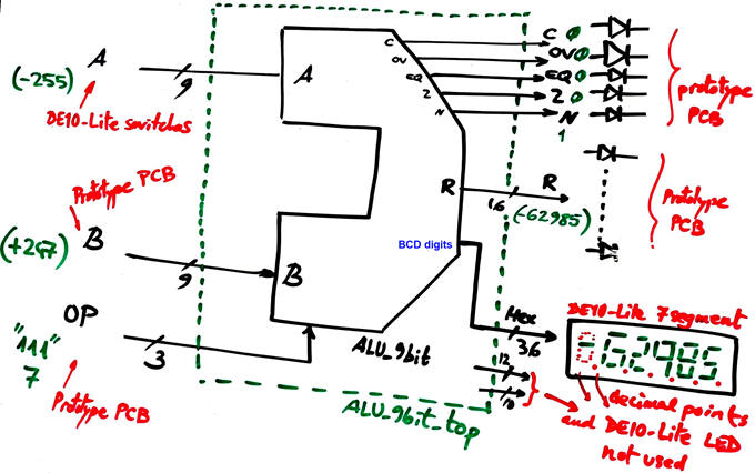
Fig. 2b. The ALU_9bit_top project implemented using the FPGA, the DE10-Lite board and the prototype resources. |
NOTE: A similar prototype can be conceived for the next Chapter II. We can run the same ALU application, replacing the switches with a 16-key matrix keypad designed as an FSM in P6 to input operands and operations sequentially, as is usual in calculators.
| Prototype specifications | Planning | Development | Test & measurements | Lab |
Planning steps are necessary for both, the ALU_9bit architecture and the auxiliary PCB.
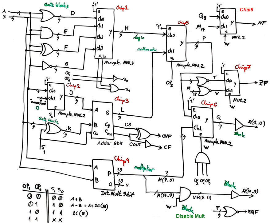
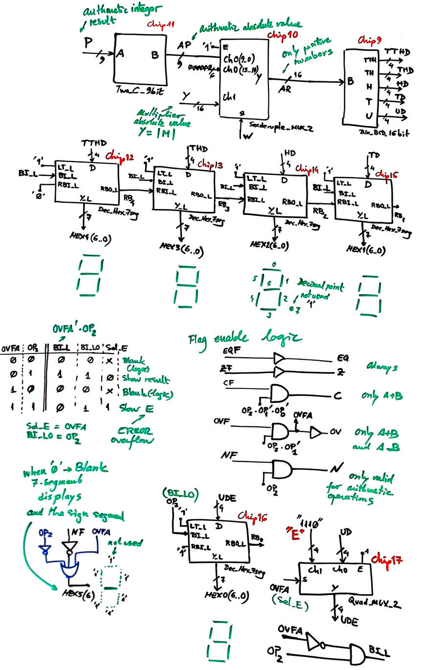
Plan C2 is required here to get an idea of the components involved and how they will be connected as a hierarchical structure. To review the theory and how components work, we can get inspiration studying similar circuits proposed in D1.18 and previous labs and tutorials. Fig. 3 shows the proposed hierarchical schematic.
Logic operations are solved by gate blocks. The Adder_9bit used for both adding and subtracting is proposed in the final Annex A1. The integer multiplier is designed in this tutorial Int_Mult_9bit. Several multiplexers select the operands, and additional logic circuits generate and enable status flags.
 |
|
Fig. 3a. Proposed ALU internal design. |
 |
|
Fig. 3b. Additional circuits for using the 7-segment displays and for enabling the flags. |
The Chip11 Bin_BCD_16bit converter for representing results in BCD will be connected to the signal Y(15..0) when performing multiplications (OP = 7), or to the signal L(8..0) when OP = 4, 5, 6. The display will be kept blank for logic bitwise operations (OP = 0, 1, 2, 3).
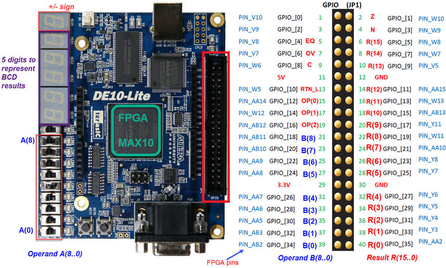
The full list of FPGA input and output connections is represented in Fig. 4. It is time to read the board's datasheet, DE10-Lite, in detail to assign FPGA pins to inputs and outputs.
 |
|
Fig. 4. FPGA connections to be used in the pin assignment tool. Board LED and other unused segments will be blanked. |
Project location:
C:\CSD\P4\ALU_9bit_top\(files)
| Prototype specifications | Planning | Development | Test & measurements | Lab |
Printed circuit board (PCB)
As indicated above, in this experiment we can use the board's switches to input A(8..0). The other operant B(8..0), the operation selector OP(2..0), the result R(15..0) and the 5 status flags (N, OV, C, Z, EQ) will be placed in an auxiliary PCB connected through the 40-pin GPIO as shown in Fig.4.
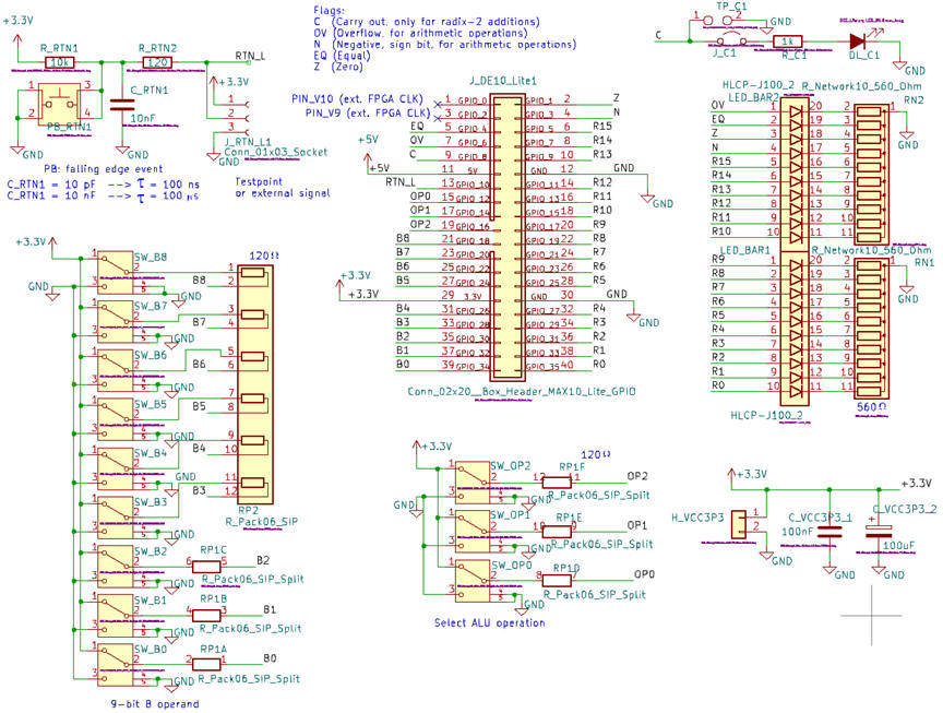
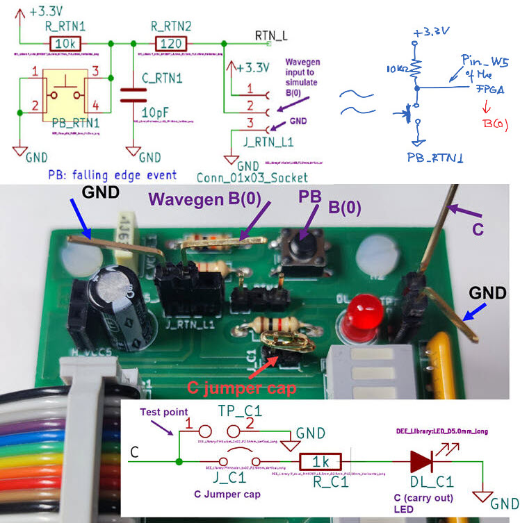
The add-on PCB design starts capturing the schematic in KiCad as shown in Fig. 5. LED bars and resistors packs can be used to save board space. A test point TP_C1 is added at the carry out (C) flag to attach oscilloscope or multimeter probes. Another header where to attach an external signal generator is placed at the push-button J_RTN_L. In this manner, we can stimulate RTN_L, assigning it, for example, to A(0), and observe waveforms at output C. Indeed, this pin-assigning step is flexible.
 |
|
Fig. 5. Schematic captured in KiCad. |
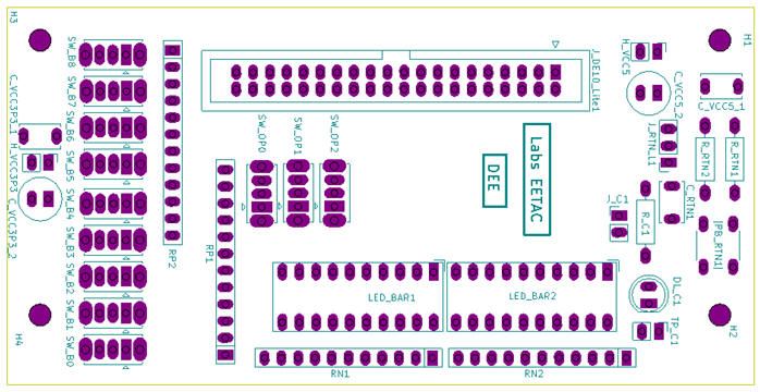
The PCB component placement is shown in Fig. 6.
 |
|
Fig. 6. PCB layout silkscreen that shows component placement and references. |
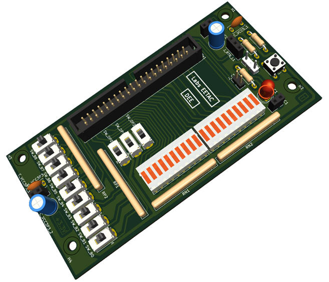
Finally, a 3D view shows the real dimensions and how the PCB will look like once soldered.
 |
|
Fig. 7. PCB 3D representation. |
Hence, once the hardware circuit for the add-on PCB is conceived, we organise a KiCad project "CSD_LAB4_PCB_v2.zip" to be able to manufacture the board. Each component contains the symbol, the footprint, and a link to the datasheet to prepare the bill of materials (BOM) spreadsheet.
NOTE: Our current CSD and DEE KiCad symbols, footprints, and 3D components are available in the library "DEE_libraries.zip" which can be unzipped and saved using these KiCad installation instructions. Basically, at this introductory PCB design level, the idea behind tuning component footprints is to enlarge their pads to make soldering easier, as shown in Fig. 8.
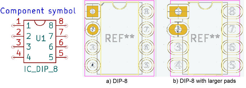 |
| Fig. 8. Example of a tuned footprint DIP-8 for easy soldering. |
Additionally, we can set several parameters for easy routing, manufacturing and soldering, such clearance between components and tracks (0.3 mm), signal (0.5 mm) and power (1 mm) track widths.
Fig. 9 shows the process of placing and soldering components on the board's prototype once manufactured using our lab machines. At this stage, we have to verify that the board works as expected or, if it is the case, make the necessary adjustments.
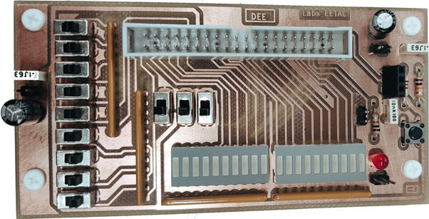 |
| Fig. 9. The idea of placing and soldering components on the PCB. |
Once this final revision step is completed, the PCB is ready for manufacturing as shown in Fig. 10.
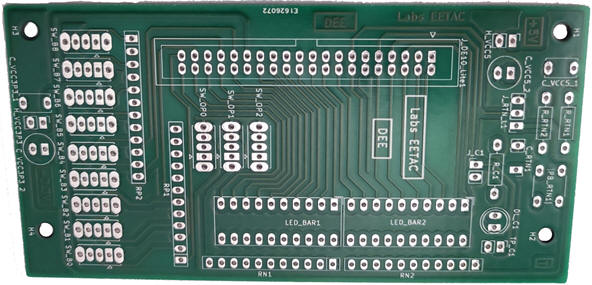 |
| Fig. 10. The final manufactured board with the silkscreen layer labels printed. |
Board's picture in Fig. 11 shows the current prototype board with all the soldered components.
 |
| Fig. 11. The idea of placing and soldering components on the PCB. The final manufactured board with the silkscreen layer labels printed. |
FPGA circuit
We can translate into VHDL the schematic "ALU_9bit.vhd" in Fig. 3a and Fig. 3b, synthesise and test the FPGA using Quartus Prime and ModelSim respectively as we have been doing hitherto. We need to take care of all the components involved in the design and include them in this plan C2 project.
These are the multiplexers used to select operands and operations: "Nonuple_MUX_4.vhd", "Nonuple_MUX_2.vhd", "MUX_2.vhd", "Quad_MUX_2.vhd", "Sexdecuple_MUX_2.vhd". All of them are implemented in a single file adapting the typical plan B Dual_MUX_4.
Annex A1 shows how to design a carry-lookahead (CLA) version of the Chip3 Adder_9bit.
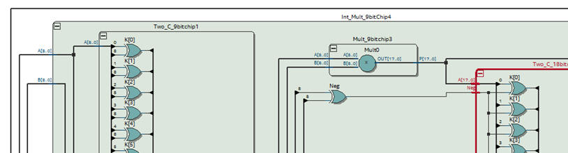
Int_Mult_9bit tutorial shows how to implement a 9-bit multiplier for integer numbers as required in Chip4.
 |
|
Fig. 12. Detail on the Int_Mult_9bit RTL (Chip4). |
Bin_BCD_16bit shows how to design the converter from radix-2 to BCD for vector size of 16-bit. You will find its top entity and its component block DM74185.
Chip9 on implementing a two's complement Two_C_9bit can be found in Int_Mult_9bit tutorial.
We can continue adding the code converters to represent the result in the six 7-segment displays. The idea is that the sign is represented as a hyphen '-' when the result is negative in the display number 5 (HEX5_L(6)). This is the decoder hexadecimal to 7-segments Dec_Hex_7seg and its block Hex_7seg_decoder that can be either plan A or plan B.
The top schematic "ALU_9bit_top.vhd" in Fig. 13 will be used to leave unconnected R16 and R17 outputs, to disable (low '0') all the DE10-Lite active-high LED and to disable ( high '1') all the decimal point segments that are not in use in this application.
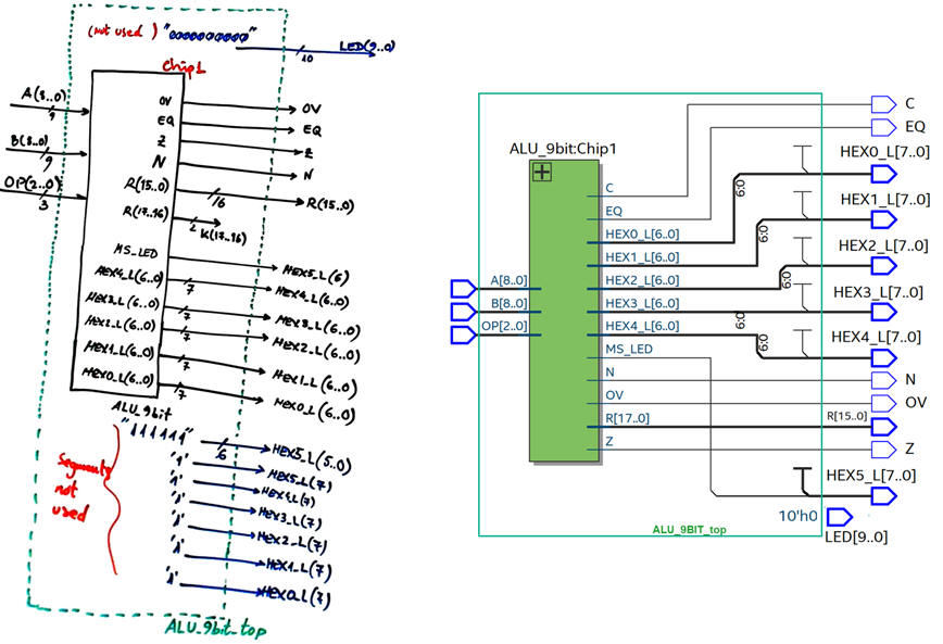 |
| Fig. 13. Top design ready for pin assignment and for prototyping. This top design allows us to add to the ALU other chip components for future experiments, such as FSM, CLK generator, data registers, etc. |
In summary, this zipped file "ALU_9bit_top.zip" contains all the VHDL files required in this hierarchical modular prototype.
Pre-lab activity #2: Start a Quartus Prime project in the planned location to synthesise the ALU_9bit application using all VHDL the files in the zip. Review the RTL and the technology schematics.
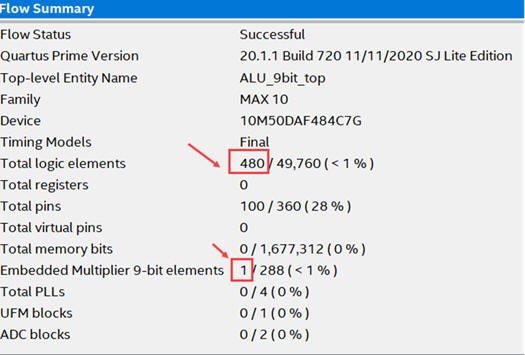
We observe how the project summary shows the use of a dedicated multiplier (one of the 288 available) and also 480 logic elements to perform logic functions. This summary gives you an initial idea of the size and complexity of the circuits that can be engineered to fit in this target chip. This ALU_9bit_top is still using less that 1% of the FPGA resources available.
 |
|
Fig. 14. Project summary. The circuit uses 480 logic elements and 1 embedded multiplier. |
| Prototype specifications | Planning | Development | Test & measurements | Lab |
ALU_9bit functional simulation
Pre-lab activity #3: Functional simulation.
It is convenient to perform a functional simulation to check that the circuit operates correctly before configuring the target chip with the programmer application. Fig. 14 shows a testbench to stimulate the circuit with operands and operations.
 |
| Fig. 14. Testbench fixture. |
This is a testbench "ALU_9bit_tb.vhd" adapted from P4 where you can adapt the stimulus process and the time constant Min_Pulse. This is the "wave.do" setup as shown in Fig. 15.
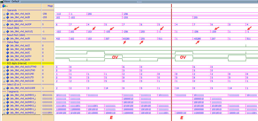 |
| Fig. 15. ModelSim simulations. Be aware that for arithmetic operations 4, 5, and 6, the result of interest is Q(8..0) or R((8..0). |
Timing analyser: longest propagation delay
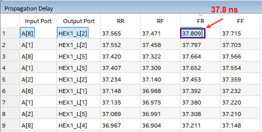
Pre-lab activity #4: Run the timing analyser to measure propagation delays as shown in Fig. 16.
Switching A(8) from high to low (F), and waiting for the HEX1_L(2) output port to go from low to high (R) takes the longest signal path, a worst-case scenario propagation delay of tP = 37.8 ns. If we attach A(8) to a signal generator, the maximum signal frequency for stimulating the circuit has to be fmax < 13.2 MHz, meaning a theoretical maximum calculating speed < 26.4 Mops (millions of operations per second).
 |
|
Fig. 16a. Propagation delay spreadsheet from input ports to output ports. |
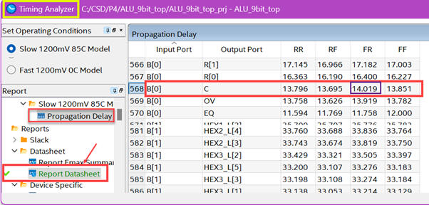
Fig. 16b shown the measurement of the propagation delay obtained attaching B(0) to the signal generator (Wavegen) and the logic analyser at the output flag C (carry out). We can visualise analogue waveforms using the oscilloscope probes and also their digitalised equivalents using logic analyser channels, as we propose to do in section F of this experiment.
 |
|
Fig. 16b. Propagation delay from input ports to output ports. |
FPGA pin assignment
Pre-lab activity #5: Adapt the ALU_9bit to the DE10-Lite and prototype resources (pins)
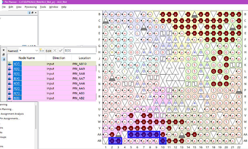
Fig. 17 shows how FPGA pins can be assigned using the Quartus Prime "Pin Planner" tool or the "Assignment editor" accordingly to Fig. 4. The information on the FPGA pins is available at the DE10-Lite user manual. The complete spreadsheet file "ALU_9bit_top_prj.csv" including all the assignments can be imported directly to Quartus before the final synthesis.
 |
|
Fig. 17. Pin Planner tool to map each circuit port to a given FPGA pin. For example, signal B(6) is connected to pin_AA9. |
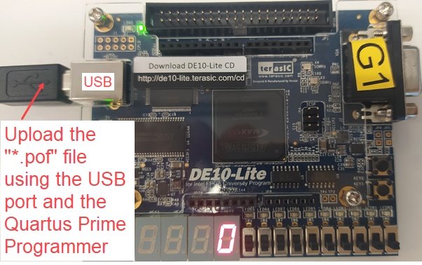
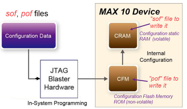
At this point in the design process, you have got the ALU_9bit_top project adapted to the DE10-Lite board ready for prototyping, experimentation and measurements. You will upload the configuration files (sof or pof) to the FPGA.
Instrument VB8012 driver installation
Pre-lab activity #6: Follow the indications to install the WaveForms software from Digilent for driving the VB8012 compact instrument in your computer.
The aim is that at least one student of your lab cooperative group will have this instrument driver installed in their PC.
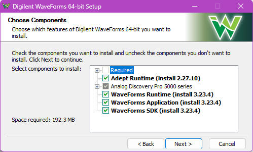 |
| Fig. 18. Instrument driver installation. |
The advantage is that you can practise with the instrument in demo mode at home, ahead of this lab session. Select the ADP5250 instrument to play with the oscilloscope, function generator, multimeter, power supplies, etc.
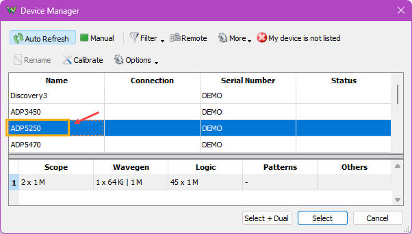 |
| Fig. 19. Instrument demo selection when the real instrument is not connected. |
For instance, choose from the waveform generator a 40% duty cycle 3.3 V digital pulse waveform. Acquire and visualise it in the oscilloscope CH1, as shown in Fig. 20.
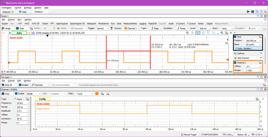 |
| Fig. 20. WaveForms windows environment. Be aware to select a light (default) background so that you can easy copy measurement pictures for your report. |
| Prototype specifications | Planning | Development | Test & measurements | Lab |
Lab session activities
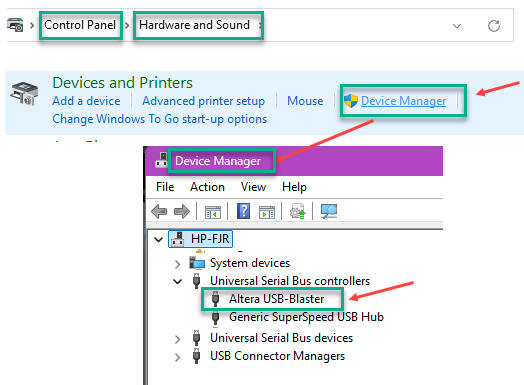
A) DE10-Lite programmer USB-blaster driver
Connect the DE10-Lite to your computer USB.
Follow the indications to install the DE10-Lite USB blaster driver in your computer if it is the first time you are using the FPGA. The aim is to allow your PC to recognise the DE10-Lite board hardware when connected as a valid USB controller as shown in Fig. 21.
 |
|
Fig. 21. Your board is correctly identified by the computer hardware device manager accessible from the control panel. |
B) Upload the FPGA configuration (programmer tool)
Firstly, to verify that the USB-Blaster driver, programmer application and board are working correctly, upload the default configuration file "DE10_LITE_Default.pof". You can also restore it after completing this laboratory. This file is copied from the board's system CD-ROM available at Terasic web.
Save your files at the same project location:
C:\CSD\P4\ALU_9bit_top\(files)
 |
|
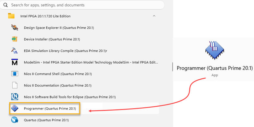
Fig. 22. DE10-Lite initial verification. This Fig. 23 shows how to reach the Programmer as an standard alone application. |
 |
|
Fig. 23. Quartus Prime Programmer. |
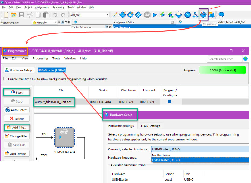
The programmer can also be accessed through Quartus Prime environment.
 |
|
Fig. 24. Programmer application launched though Quartus Prime development environment. |
Secondly, we like to write the configuration flash memory (CFM) of the FPGA and make the circuit permanent (not erased when unplugging the board) "ALU_9bit_top.pof". Save the file at the same project location.
NOTE: Alternatively, this is the volatile final FPGA "ALU_9bit_top.sof" configuration file to be used directly by the Quartus Prime programmer. The extension .sof stands for SRAM Object File, thus, the FPGA configuration disappears when unplugging or disconnecting the board from the power supply.
 |
|
Fig. 25. FPGA configuration memories. |
C) Run the circuit and test operations
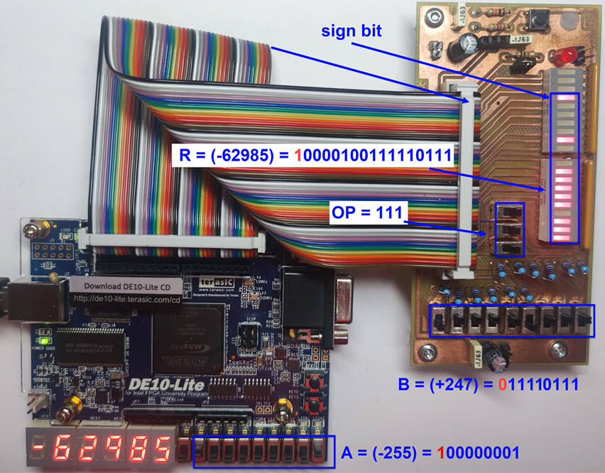
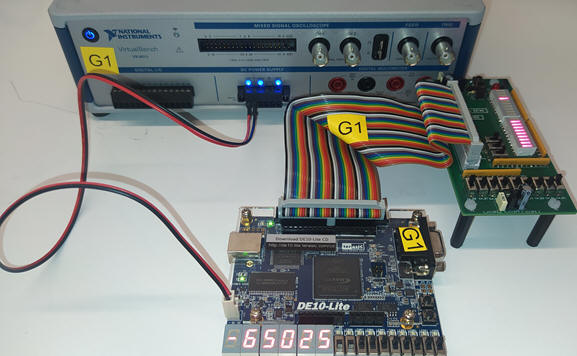
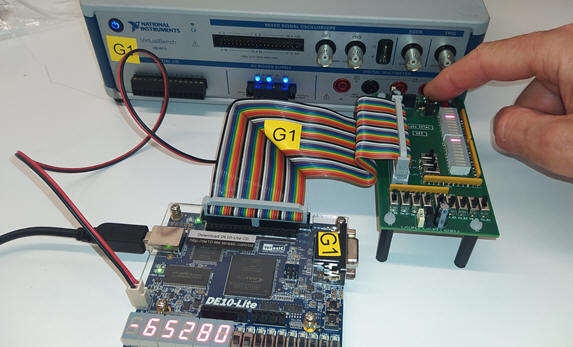
Unplug the USB cable and attach using the 40-pin flat cable the prototype board to the DE10-Lite. Connect again the USB interface to power the board with VCC = 5 V.
Fig. 26 shows the prototype performing an operation. Apply several input vectors and annotate outputs when performing logic and arithmetic operations, as a way to verify your pre-lab activity #1.
 |
|
Fig. 26. Prototype connecting the inputs and outputs add-on board to the DE10-Lite training board ready for running the truth table. An example of signed multiplication is visualised. |
And from now on, with our prototype verified and operating correctly, we are ready to perform laboratory measurements using the compact VB8012 instrument to observe additional circuit features. We can characterise the circuit's performance as if we had to write a kind of datasheet or technical report to accompany the product.
In this experiment, we will measure static power consumption, propagation delay for a given input/output propagation path (from B(0) to flag C) and dynamic power when working at high speed.
D) Static power consumption
Static power
PS = VCC · ICC
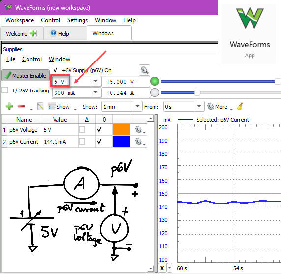
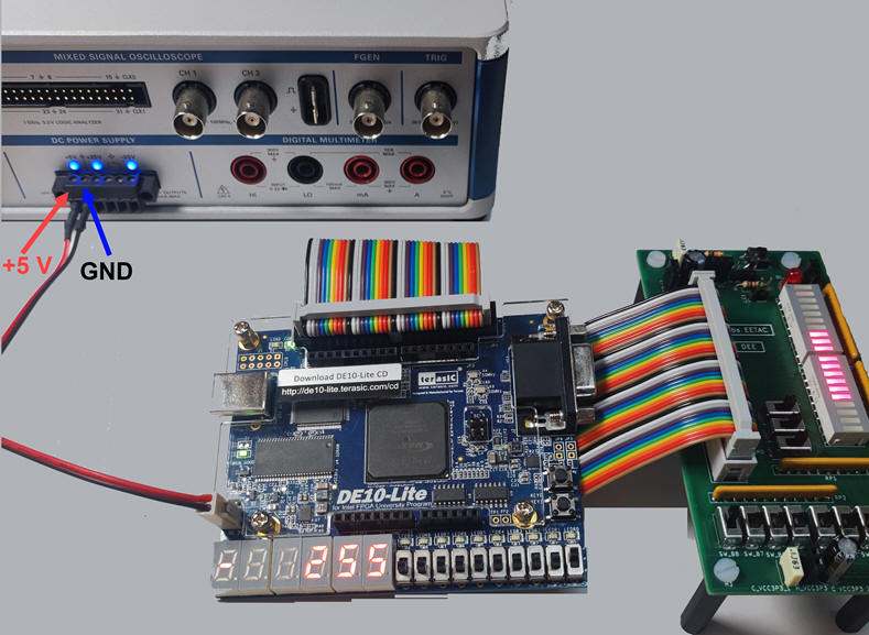
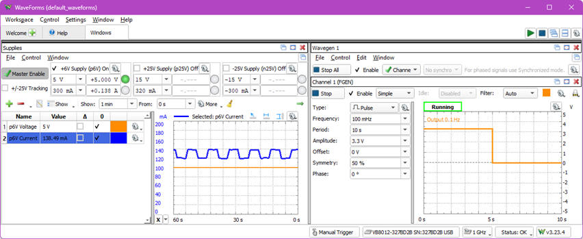
Connect the instrument VB8012 to the PC USB, run the WaveForms app and screw the power supply cable as shown in Fig. 27. The DE10-Lite board will be powered from the instrument, and its USB will be used only for uploading the FPGA configuration.
    |
|
Fig. 27. The VB8012 p6V power supply adjusted to +5 V to drive the board, replacing the power supply from the USB cable. Voltage and current readings will be available. |
Determine the static power consumption PS (mW) for various ALU operations. The measurement accounts for the power consumed by the FPGA, all other chips on the board, and the power required to illuminate the LED segments that display the results.
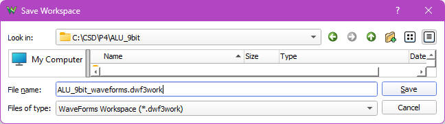
The WaveForms setup workspace (file extension: "*.dwf3work") may be saved as an additional file in the project folder, as shown in Fig. 28. For example: default_ps_D.dwf3work.
 |
|
Fig. 28. Saving the WaveForms Workspace setup in the project folder. |
E) Propagation delay measurement
Let us characterise the speed of some internal circuits, such as the Chip3: Adder_9bit, which has the C (carry out) output connected to the prototype's test point pin TP_C1.
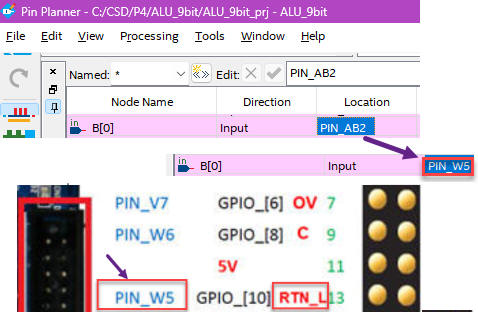
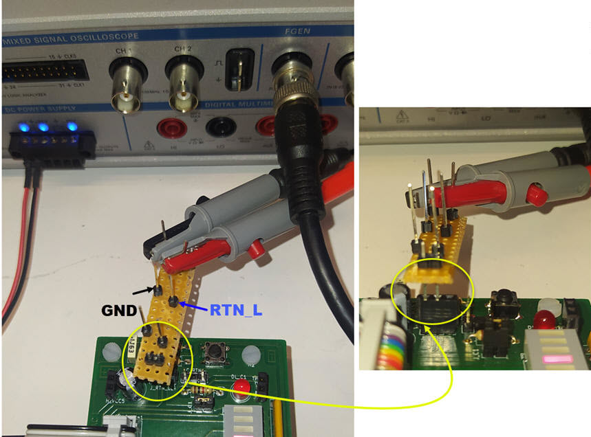
To carry out this measurement, the only hardware modification required is to reassign the pin B(0) from the switch at pin_AB2 to the push-button RTN_L at pin_W5. Do this new reassignment in the Quartus Prime Pin Planner and re-synthesise the project. This is the new assignment file "ALU_9bit_top_prj_E.csv". These are the new modified FPGA "ALU_9bit_top_E.sof" and "ALU_9bit_top_E.pof" configuration files to upload, where the B(0) signal is wired to the RTN_L input pushbutton (pin_W5).
 |
|
Fig. 29. Using the Pin Planner app to reassign the B(0) from the switch to the RTN_L push-button. |
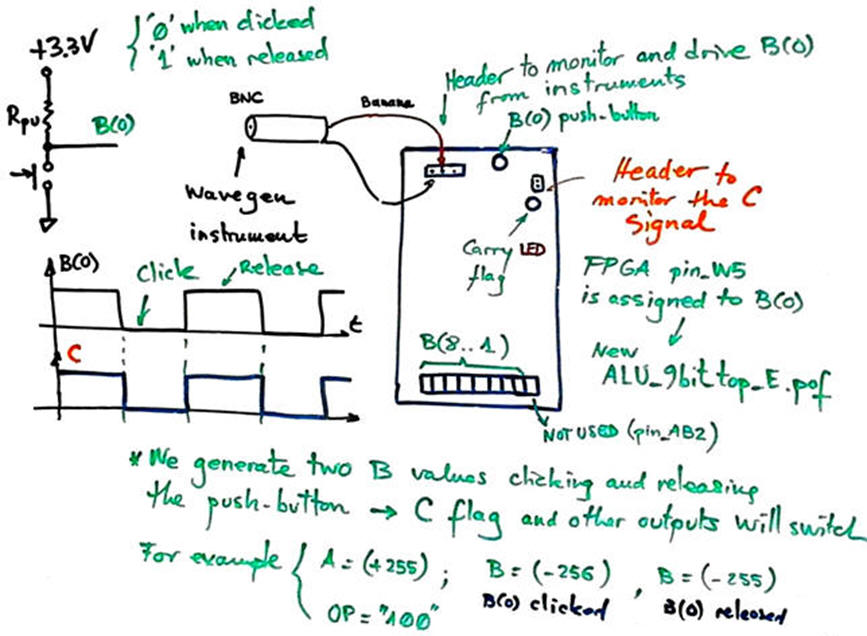
Program the FPGA and check that B(0) is asserted when clicking the push-button RTN_L as shown in Fig. 30. Pressing and releasing the push-button B(0) is like executing two truth table combinations.
  |
|
Fig. 30. Clicking B(0) push-button generates a '0', releasing the push-button generates a '1'. |
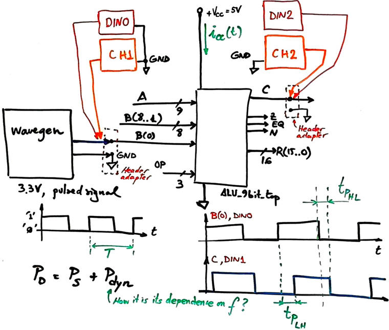
Therefore, to automate this stimulus process, we will drive B(0) with the function generator Wavegen connected to the header by means of a BNC-banana cable. The C output is also wired to another header.
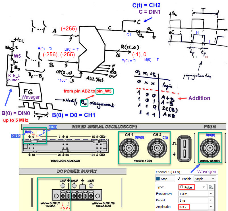
We can make the connections and use the operands represented in Fig. 31. The ALU_9bit uses C as an internal signal to calculate the OV flag, as shown in Fig. 3b.
To carry out this OP = "100" experiment, let us choose two convenient integers A and B. The board's push-button RTN_L will replace the B(0) switch to be able to drive signals using a function generator.
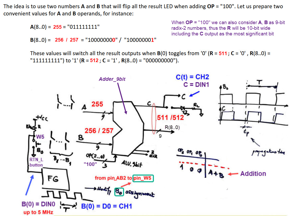
The idea is to use two numbers A and B that will flip all the result LED when adding OP = "100" (R = A + B), for instance:
A(8..0) = (+255) = "011111111"
B(8..0) = (-256) = "100000000" ; B(8..0) = (-255) = "100000001" (Driving B(0) with a 3.3 V pulsed wave)
These operand values will switch all the result outputs when the function generator toggles B(0):
---> B(0) = '0' ---> (+255) + (-256) = "111111111" = R(8..0) ==> (-1), C = '0'
---> B(0) = '1' ---> (+255) + (-255) = "000000000" = R(8..0) ==> ( 0), C = '1'
 |
|
Fig. 31. Driving B(0) with a square wave (pulse) from the function generator Wavegen. In the same way, other output signals can be reassigned to the C header to measure for example the multiplier Mult_9bit propagation delay. |
Alternatively, for this experiment, and only for adding (OP = "100") we can also imagine the operands as radix-2 numbers. The experiment will be the same, as we simply like to switch all the result bits, driving a single input B(0) from the Wavegen.
In this way, we can visualise the internal Adder_9bit (and other auxiliary circuits in the path) propagation delay from B(0) to C on the logic analyser and oscilloscope. The parameter of interest is the Wavegen maximum frequency fMAX that can be applied to the circuit.
To facilitate the connection of several instruments and probes, you can use the adapters plugged on the test point sockets TP_C1 and J_RTN_L1 as shown in Fig. 32.
  |
|
Fig. 32. We will use male pins for both: drive B((0) externally connecting the instrument function generator Wavegen, and for monitoring the carry out (C) LED value. Place the J_C1 jumper cap on the male pins to connect the LED DL_C1 to visualise the C signal. |
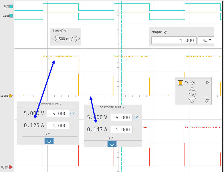
Let us connect the Wavegen with a 1 Hz, 50% symmetry, 3.3 V pulse signal using the cable BNC-male to banana with two alligator clips. Check that the C LED toggles as previously when pressing the push-button with fingers.
 |
|
Fig. 33. Connecting the Wavegen to drive B(0) using a BNC-male to two alligator clip cable. |
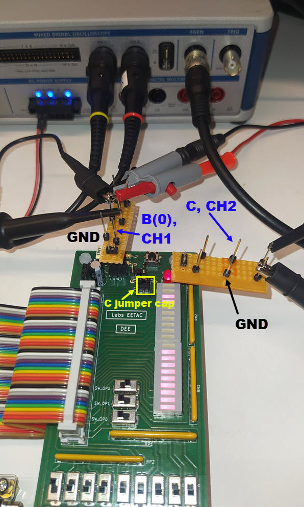
From now on, we can play modifying the signal frequency. Hence, let us visualise waveforms in the oscilloscope (CH1 --> B(0), CH2 --> C). In this fashion, we can measure the propagation delay using cursors and two oscilloscope channels. Adjust the probes attenuation 10X, and 2 V/div.
 |
|
Fig. 34. CH1 and CH2 oscilloscope probes. |
However, it is much better to digitalise these signals using the logic analyser instrument. Hence, let us add the digital signals DIN0 ---> B(0), CH1; and DIN1 ---> C, CH2. Keep the circuit layout clean, bending and setting aside the probes of no interest.
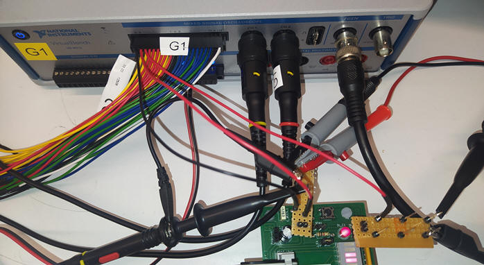  |
|
Fig. 35. Using probe adapters simplifies connections and keep the experiment clean. |
 |
|
Fig. 36. Two digital channels (DIN 0 and DIN 1) and two probes for the analogue channels CH1 and CH2. |
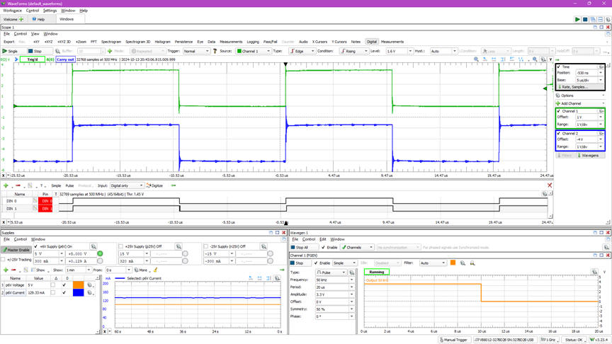
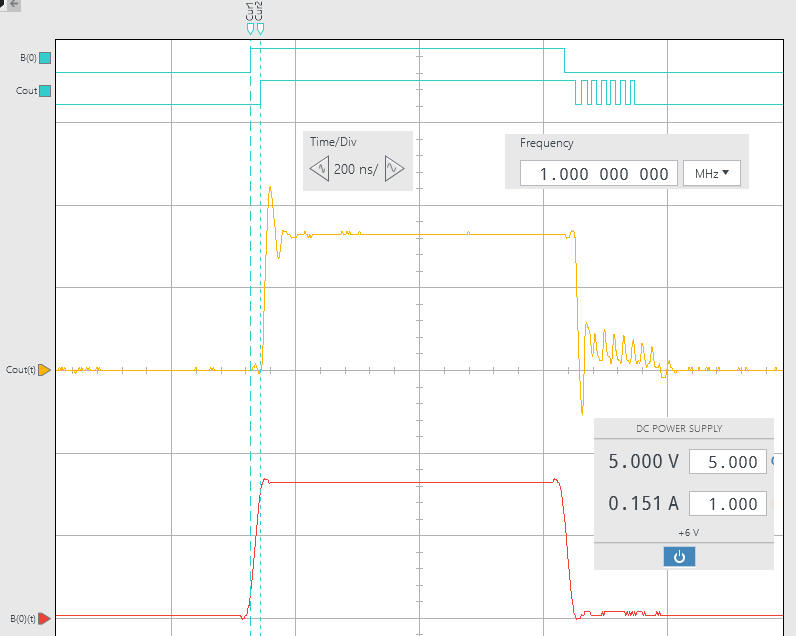
Compare and discuss your lab results with measurements from Quartus Prime timing analyser in Fig. 16.
The next picture Fig. 37 shows example printed waveforms with time cursor measurements. Discuss their validity or try different frequencies and configurations to see in which way the measurements makes more sense.
 |
|
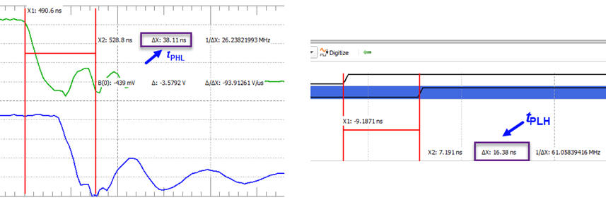
Fig. 37. Propagation delay tPHL and tPLH measurements examples using both analogue and digital signal acquisitions in this given signal transition. |
Overshoot, sinusoidal ringing or damping and noise are appreciated at the oscilloscope signals at higher frequencies. Thus, the digital acquisition at 1 GS/s (1 ns resolution) captures this noise as extra digital pulses (signal bouncing). It is clear that long flat cables and standard probes do not allow much higher frequencies. Therefore, is it possible to attain the theoretical fMAX using our instrument setup?
How to get rid of signal bouncing and condition perfect digital signals can be studied in other experiments. In our projects, we can add an specialised digital Debouncing filter or even use commercial chips attached to push-buttons. If you disconnect the Wavegen, can you capture the waveform transients when clicking the push-button RTN_L?
F) Dynamic power consumption
PD = PS + Pdyn
The objective is to measure the power consumption at several operating frequencies. For instance: 1Hz, 10 kHz, 1 MHz or other values such 5 MHz or 10 MHz.
Measuring total power consumption firstly at 1 Hz and secondly at 1 MHz (PS + PD = 755 mW), we can deduce the dynamic power of the FPGA chip at such frequency of operation PD = 85 mW.
  |
|
Fig. 38. Power consumption at 1 Hz and 1 MHz. |
Note: Before finishing the lab session, using the Programmer, you can restore the configuration flash memory (CFM) of the DE10-Lite board to its original default application saved in this unit DE10-Lite.
NOTE : A prototyping PCB board like this one expanding the DE10-Lite resources with many more input and outputs, once manufactured, can be used for other laboratory projects such counters, shift registers, etc. We just need to rename the wires in the KiCad schematic and reassign FPGA pins.
Annexes
Annex A1. Adder_9bit
Example of planning the Adder_9bit required in this project. We use the carry lookahead architecture already presented in LAB4_1 example: Adder_16bit.
 |
|
Fig. A.1.1. Adder_9bit symbol and truth table. |
We can invent and translate it as with other similar circuits: using plan C2 annotating all the signals and chips.
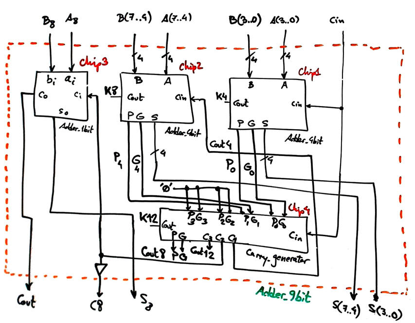 |
|
Fig. A1.2. Proposed Adder_9bit. |
This is the VHDL translation of the Fig. 2 schematic: Adder_9bit.vhd. This is the component Adder_4bit CLA that also includes the Chip2 Carry_Generator. This is the Chip3 Adder_1bit based for instance in plan A equations.
Annex A2: Signal integrity
Optional (out of the CSD scope). At this level, many more questions may be asked regarding results and waveforms from these experiments. For example:
- What is the effect of the long flat cable? What kind of circuit is required to drive digital signals over long wires?
- What kind of improvements can you imagine for your instrumentation testbench What kind of instruments and adapters professional companies use to characterise their integrated circuits and products?
- How to drive the same B((0), repeating the same experiments using an internal CLK signal that will probably generate clearer digital waves? Fig. A2.1 shows the experiment when using an internal CLK_Generator (from lecture L8.2). This is the full experiment in case you like to try it in the lab: "ALU_9bit_top_CLK.zip".
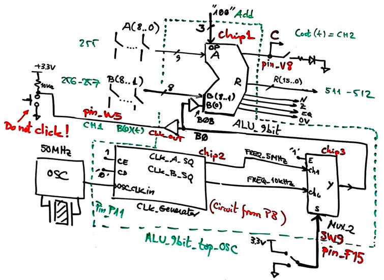 |
| Fig.A2.1. Let us measure the circuit performance when using an internal CLK signal instead of the external VB8012 function generator. Let us see whether we can obtain clearer waveforms. B(0) used as output is available at the same pin W5 to be monitored at the oscilloscope CH1. |
And, after this initial question, many more advanced ones appear. For instance:
- How to design the PCB and the instrument probe setup so that signal bouncing, noise and ringing can be reduced or even eliminated to maintain signal integrity?
| Home Term 26/27-Q1 Contact Products Electronic devices and companies Software Books Magazines Instruments DEE Library EETAC DEEL |

|
|
| Web activa des de 09/2001, @ F. J. Robert, Web editat amb Microsoft Expression Web 4. El contingut és un complement als materials d'estudi del curs Circuits i Sistemes Digitals disponibles al campus digital Atenea. Llicència:Reconeixement 4.0 Internacional de Creative Commons |