|
|
Bachelor's Degree in Telecommunications Systems and in Network Engineering |
|
|
Installing KiCad and customised libraries |
||
![]()
Let us follow several steps to install KiCad and start a project copying and adapting from another sample project. Try to avoid starting your projects from scratch as it is quite complicated and entertaining. Besides, after long training sessions you will certainly end fixing some parameters and constrains for most of your designs. Thus, in CSD and DEE this initial setup is already done and ready to use; you will find several introductory example PCB for students and hobbyists.
The key idea is to let KiCad upgrade as soon as new versions are available, and at the same time, keep our libraries secured and organised always in the same folders.
1. KiCad installation
Download the software and proceed with a typical installation.
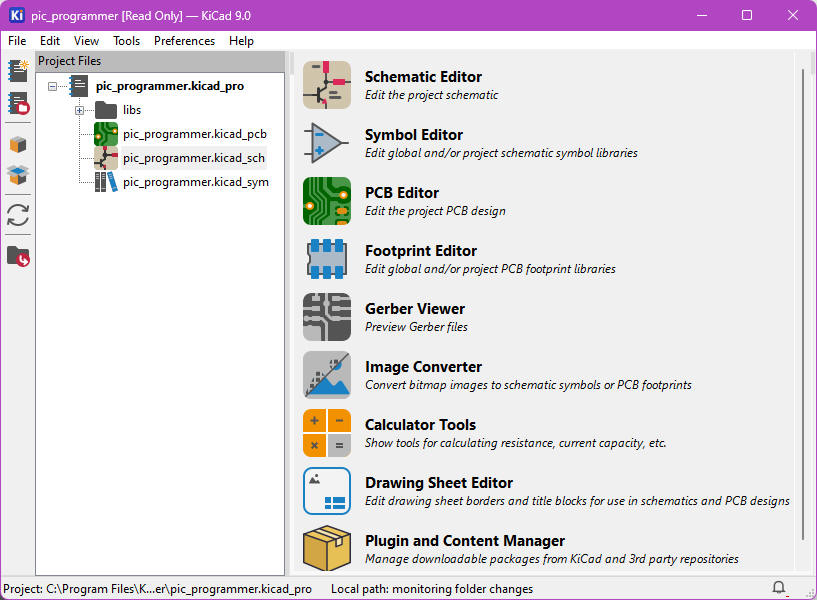 |
Fig. 1. Software KiCad and a typical project. |
Now that you have completed the installation you can browse several example projects. Check that you can open the schematic, the PCB and also its 3D view.
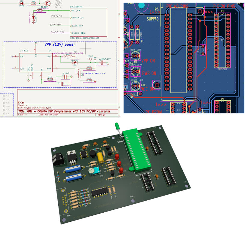 |
Fig. 2. Example project from KiCad: schematic, PCB and 3D views. |
2. Copy the custom symbol library DEE_Symbols.kicad_sym
Let us unzip the DEE_libraries.zip file and copy our customised symbols library DEE_Symbols.kicad_sym to the indicated directory. Configure the location relative to the environment variable KICAD_DEE_LIBRARIES as shown in Fig. 3.
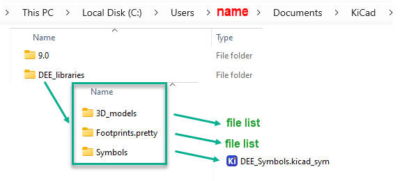 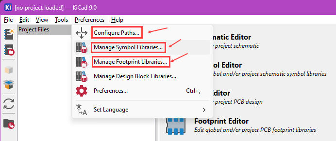 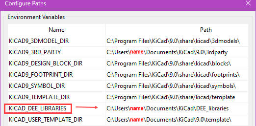 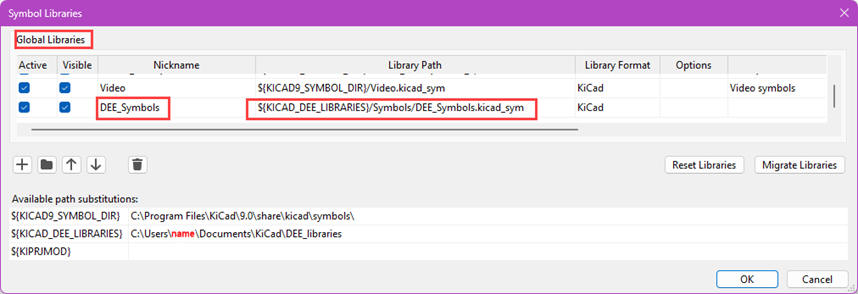 |
Fig. 3. This is the folder location for our DEE_Symbols library once the environment KICAD_DEE_LIBRARIES variable is added. |
3. Copy the custom Footprints.pretty library
Let us unzip and copy our customised footprints library Footprints.pretty. Make it it relative to the same environment variable.
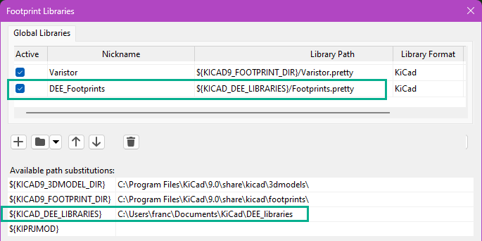 |
Fig. 4. This is the folder location for our Footprints.pretty library. The library nickname is DEE_Footprints |
4. Copy the custom 3D models library DEE
Let us unzip and copy our customised 3D models library to the 3D_models folder. Make it it relative to the environment variable. 3D models are associated to components as another footprint property. They are visualised using the 3D view window.
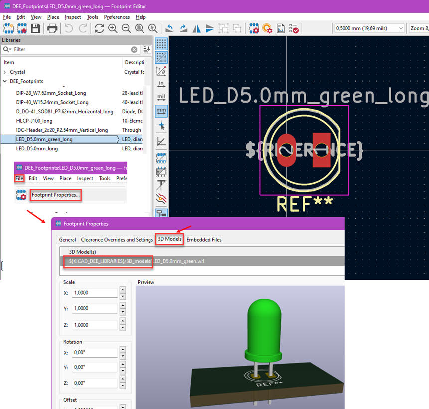 |
Fig. 5. This is 3D_models folder location for our 3D models library. |
5. Start a new project copying and adapting from one of our samples
For example, to start our own projects, we can imagine a GPIO expansion prototype to be connected to the DE10-Lite board through the expansion connector and a 40-pin flat cable. We add nine switches, one push-button and an array of seventeen LED. We enumerate these components continuing DE10-Lite references. We can use several tuned symbols, footprints and 3D models. Specially long pads for easy soldering. This is the full project GPIO_EXP.zip.
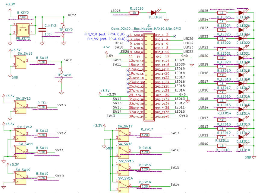 |
Fig. 6. GPIO schematic capture and FPGA pins assigned through the 40-pin expansion header. |
 |
Fig. 7. FPGA pin assignments. |
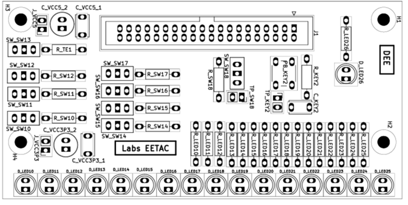 |
Fig. 8. PCB silkscreen showing component placements. |
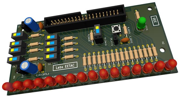 |
Fig. 9. 3D view showing the 3D models attached to components' footprints. |
From now on you can copy and adapt your design. The key idea is to go step by step modifying only one or very few components at a time, running ERC and keeping zero errors and zero warnings while working in your project. Keep the three, schematic, PCB and 3D synchronised.
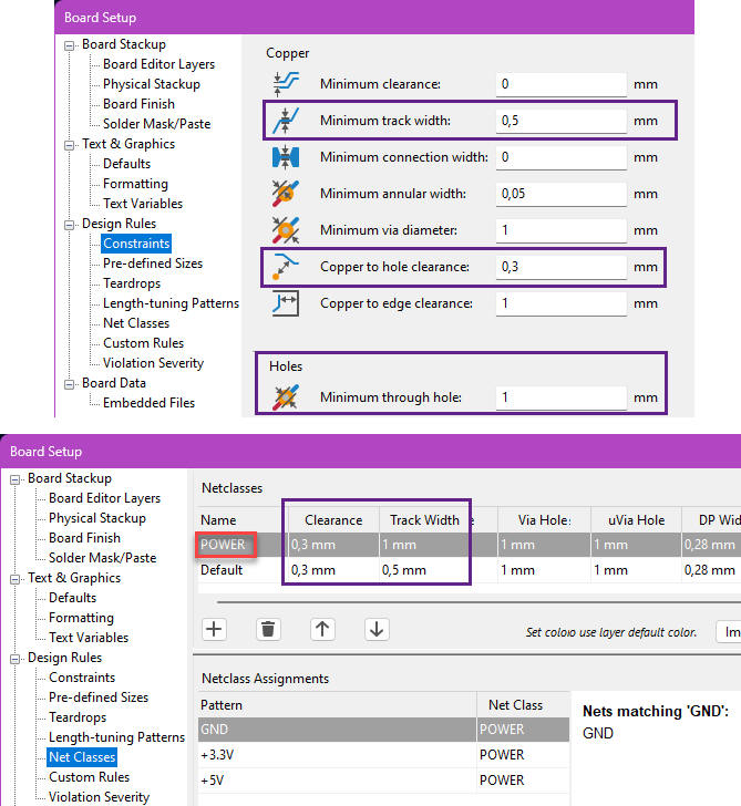 |
Fig. 10. Some important board parameters. |
6. Useful KiCad tools for updating or changing components
You can massively change symbols library links using the tool shown in Fig. 11. As beginners, we recommend to use only global KiCad symbols and your own modified ones, stored in our symbols library indicated in Fig. 3.
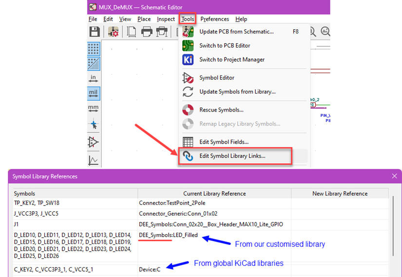 |
Fig. 11. Modifying symbol libraries. |
You can massively update or modify footprints using the tool:
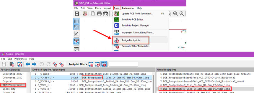 |
Fig. 12. Modifying footprint libraries. |
You can maintain your customised 3D models using the footprint editor tool, and clicking footprint properties.
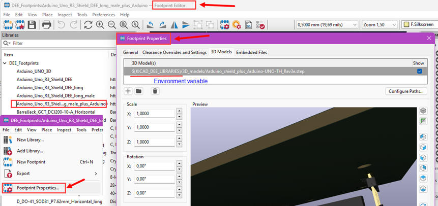 |
Fig. 13. Assigning 3D models to customised footprints. |
| Home Term 26/27-Q1 Contact Products Electronic devices and companies Software Books Magazines Instruments DEE Library EETAC DEEL |

|
|
| Web activa des de 09/2001, @ F. J. Robert, Web editat amb Microsoft Expression Web 4. El contingut és un complement als materials d'estudi del curs Circuits i Sistemes Digitals disponibles al campus digital Atenea. Llicència:Reconeixement 4.0 Internacional de Creative Commons |