|
|
Bachelor's Degree in Telecommunications Systems and in Network Engineering |
|
|
|
||
|
|
Adder_4bit carry-lookahead. Plan C2: hierarchical multiple-file VHDL |
|
|
|
||
Type 74HCT283
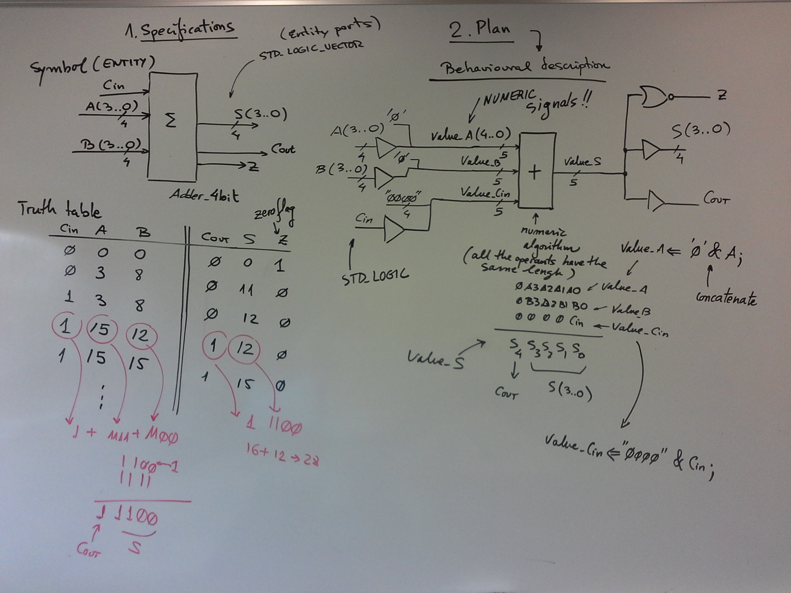
1. Specifications
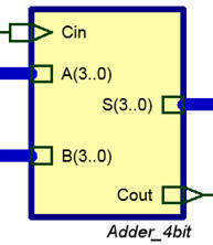
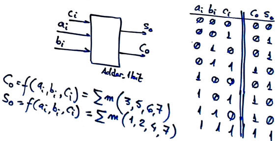
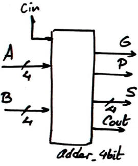
Design a 4-bit adder (Adder_4bit) using the carry-lookahead (CLA) technique in a hierarchical structure of multiple VHDL files. In Fig. 1 there is the circuit's symbol and truth table. The algorithm is: S = A + B + Cin. The commercial 4-bit adder standard chip 74HCT283 is similar.
 |
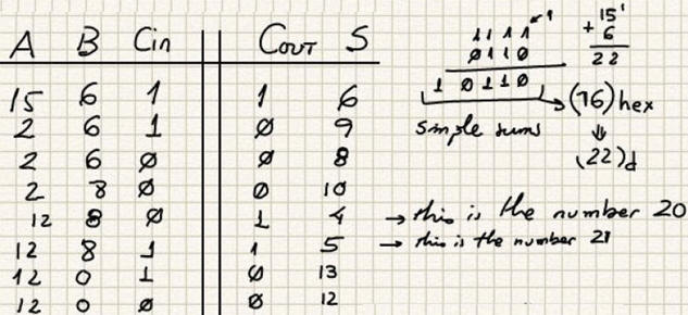 |
| Fig. 1. Adder_4bit symbol and truth table. | |
Fig. 2 shows an example of timing diagram.
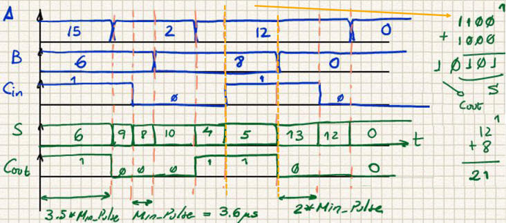 |
| Fig. 2. This is an example of a timing diagram representing some operations. |
The idea of the carry-lookahead to reduce the propagation time in addition operations is explained in Wikipedia and also in many books. For instance: Ercegovac, M., Lang, T., Moreno, J. H., "Introduction to Digital Systems", John Wiley & Sons, 1999). It includes slides: Chapter 10 is on arithmetic circuits.
2. Planning
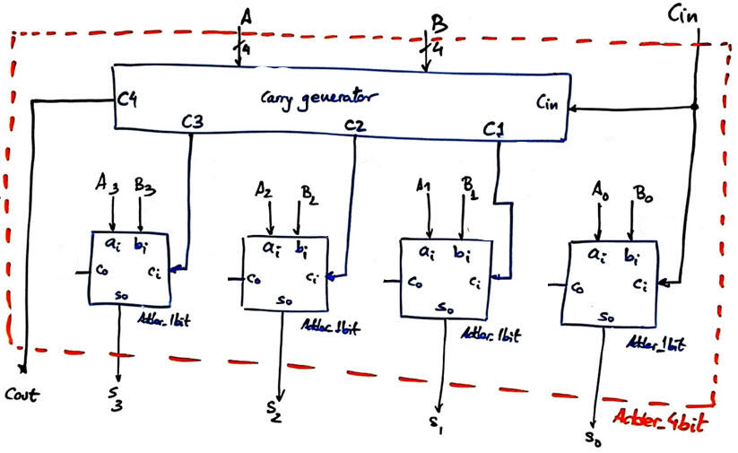
In this project we will imagine that all the carry signals are generated with the same propagation delay by the additional component Carry_generator. Therefore, a structural and hierarchical plan C2 based on the carry-lookahead technique is required, as it is shown in the sketch from the Wikipedia entry or from any book on digital circuits.
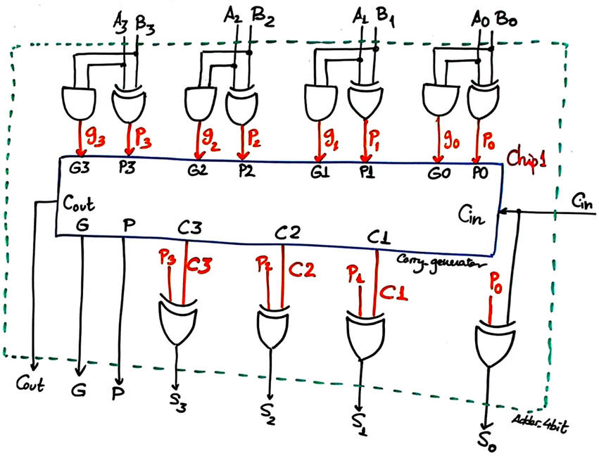
Fig. 3 schematic shows that NGL = 6. Therefore, this architecture reduces the circuit's propagation time to tP = 6·tPg instead of tP = 12·tPg as is was the case in the ripple-carry (RC) Adder_4bit.
|
|
Fig. 3. The CLA initial idea: adding more resources to synthesise an extra circuit Carry_generator to obtain the four carries C(4..1) required by the Adder_1bit chips in a single step. In this way, NGL = 6. |
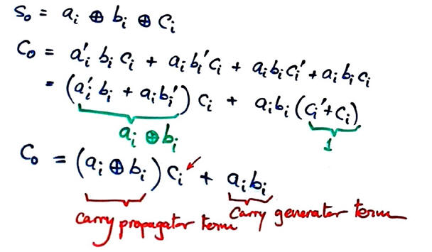
At this point, we have room for further optimisation to try to obtain the same functionality using less resources. We observe in Fig. 3 that the Adder_1bit circuit do not need to be a full 1-bit adder because the logic for Co is not used but replaced by the new circuit Carry_generator. Hence, it can be simplified.
And, at the same time, we can focus our attention on how the equation Co = f(ai, bi, ci) is written in algebra.
|
|
| Fig. 4. Adder_1bit symbol and truth table. |
|
|
Fig. 5. The idea of carry propagator (pi) and carry generator (gi) in the 1-bit adder unit. |
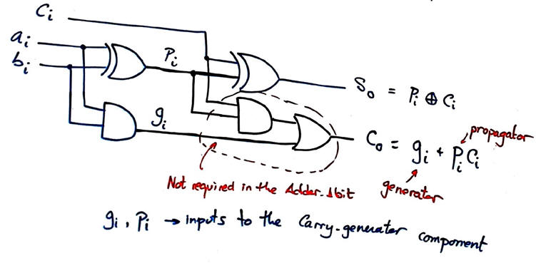
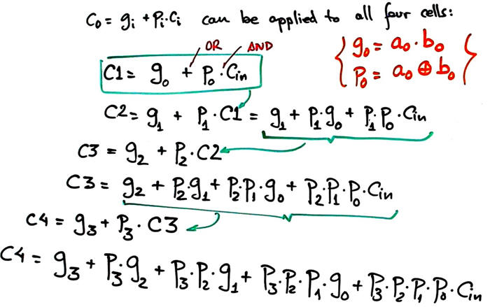
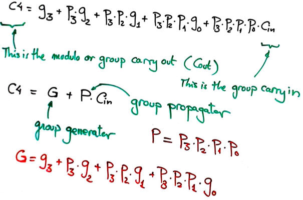
Thus, Carry_generator output equations for the four Adder_1bit units can be deduced as shown in Fig. 6. All of them consisting of only two levels of gates. Note that in this circuit, the NOT literals are not required.
|
|
Fig. 6. Carry_generator equations. |
To be able to chain Adder_4bit when constructing larger adder structures, we must pay attention to the final Cout, it can also be explained in terms of group or module propagator (P) and generator (G).
 |
 |
|
Fig. 7. Outputs group propagator (P) and group generator (G) will be included in the symbol so that this Adder_4bit will be chainable along with other levels of carry generator components. For instance, read in Wikipedia how an Adder_16bit works. |
|
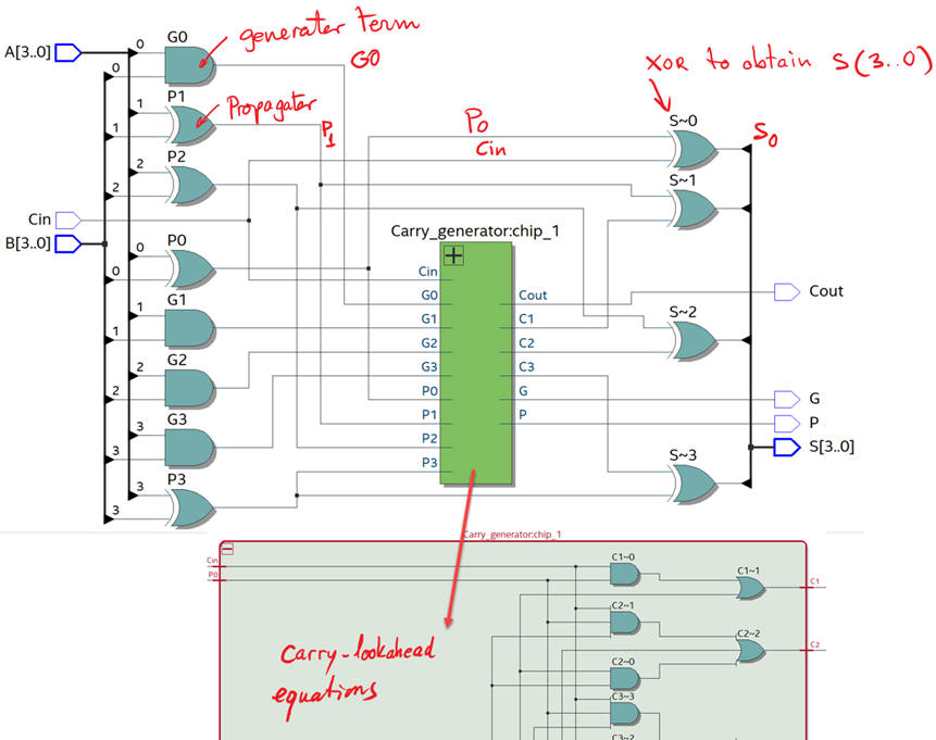
In this way, the circuit idea in Fig. 3 can be optimised as shown in Fig. 8, containing only the component Carry_generator and logic gates. From the equations, we observe that the circuit's propagation time is reduced to tP = 4·tPg.
|
|
Fig. 8. Optimised internal architecture for the CLA Adder_4bit. Two VHDL files will be required. NGL = 5. |
Project location:
C:\CSD\P3\Adder_4bit_CLA\(files)
3. Developing the project using EDA tools
Fig. 8 schematic is translated into VHDL as Adder_4bit.vhd, along with the component Carry_generator.vhd.
Considering the Fig. 8 circuit, we can pick up as target chip an Intel PLD, for instance the MAXII EPM2210F324C3 and develop a multiple file project as shown in the Fig. 9 RTL schematic.
|
|
|
Fig.9. RTL view of the hierarchical structure once synthesised using EDA tools. It looks like as expected from Fig. 8. It is somewhat similar to the classic 74HCT283. |
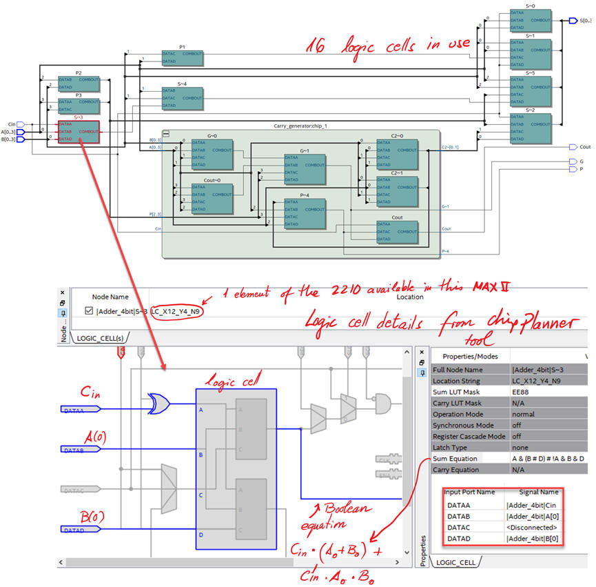
In MAX II CPLD devices, logic gates and circuits are synthesised using logic elements.
|
|
|
Fig.10. Technology view when using a MAXII CPLD . How many logic elements are used? This view and the project summary tell us that 16 logic elements are used. |
4. Testing and validating the design
The testbench fixture allows us to perform VHDL simulations for testing the unit-under-test.
|
|
|
Fig.11. VHDL testbench fixture. |
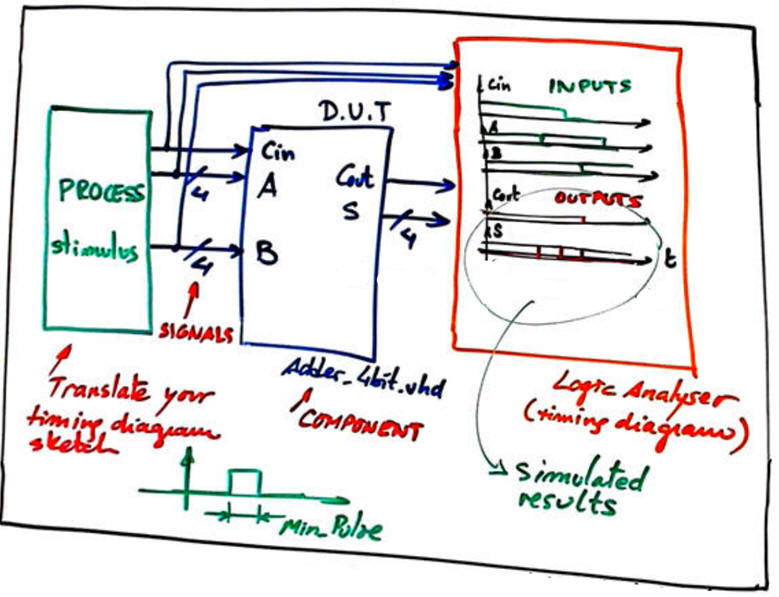
Translating the testbench into VHDL "Adder_4bit_tb.vhd", we can run the VHDL simulation EDA tool to obtain and discuss the timing diagram. This is an example of resulting waveforms.
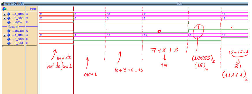 |
| Fig. 12. Example of a test results. |
5. Testing (gate-level)
The same VHDL fixture used in the functional simulation in Fig. 11 applies for this gate-level testbench because the unit under test (UUT) is the same.
|
|
|
Fig.13. Gate-level measurements in a given signal transition for measuring propagation times. |
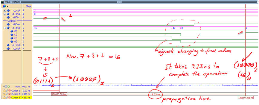
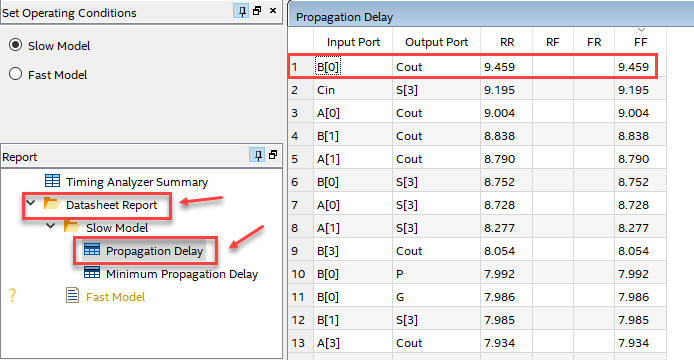
Timing analyser spreadsheet will show us the worst-case scenario, the longest propagation delay, and thus, the maximum speed of the circuit.
|
|
|
Fig.14. Timing analyser results. In this example the longest signal propagation path is from B(0) to Cout, representing tP = 9.46 ns. From this measurement we can deduce what is the maximum frequency of operation (representing the minimum value for Min_Pulse, or the maximum ratio at which inputs can be switched) for a given target chip. In this case speed = 1/tP = 105.7 Mops (Millions of operations per second). |
It is time to compare both implementations of the same circuit (1) ripple-carry Adder_4bit and (2) CLA Adder_4bit studied here. Which one is faster? Which one uses more resources?
For instance, in LAB4_1 a project of 16-bit adder is discussed comparing performances when designed using a ripple-carry and carry-lookahead architectures.
6. Report
Follow this rubric for writing reports.
6. Prototyping
Use training boards and perform laboratory measurements to verify how the circuit works.
|
|
Other materials of interest
(optional) Plan B.- Behavioural. It is too complex and difficult to explain and systematise for the learning goals of this introductory CSD course). This is the same circuit where the truth table itself (behavioural description) has to be written in VHDL using this sketch. (A single VHDL file project). The VHDL file will be named "Adder_4bit.vhd". This is another shorter version of the same file "Adder_4bit.vhd", simply to show you the flexibility of the description language. Fig .15 represents the RTL of the flat -behavioural- architecture.
Represented in Fig. 15 is the RTL of the flat (behavioural, algorithmic) architecture.
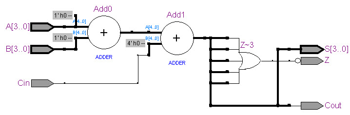 |
Fig. 15. RTL schematic from a behavioural (algorithmic, high-level, truth table) point of view. |
| Home Term 26/27-Q1 Contact Products Electronic devices and companies Software Books Magazines Instruments DEE Library EETAC DEEL |

|
|
| Web activa des de 09/2001, @ F. J. Robert, Web editat amb Microsoft Expression Web 4. El contingut és un complement als materials d'estudi del curs Circuits i Sistemes Digitals disponibles al campus digital Atenea. Llicència:Reconeixement 4.0 Internacional de Creative Commons |