|
|
Bachelor's Degree in Telecommunications Systems and in Network Engineering |
|
|
|
||
|
|
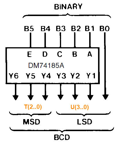
6-bit binary radix-2 to BCD converter |
|
|
|
||
Plan B: behavioural (high-level) single-file VHDL (flat)
1. Specifications
Design a 6-bit binary radix-2 to BCD converter as explained in Fig. 1, adapting to VHDL the circuit from the DM74185 datasheet using plan B behavioural approach.
The annex at the page bottom includes the design of the DM74185 block functionality to be used for expanding similar circuits to a larger number of bits.
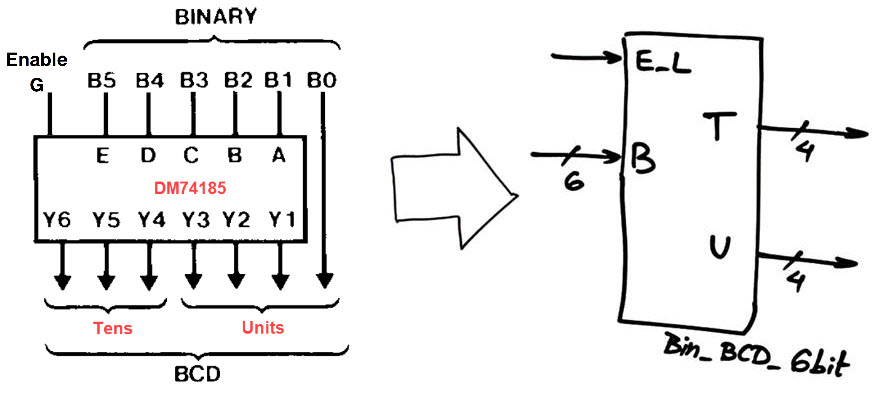 |
| Fig. 1. Bin_BCD_6bit symbol adapted from the chip DM74185. When the chip is disabled, we will implement the code 'dd'. |
Our circuit can be implemented adapting the datasheet truth table.
 |
|
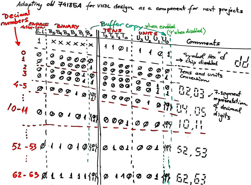
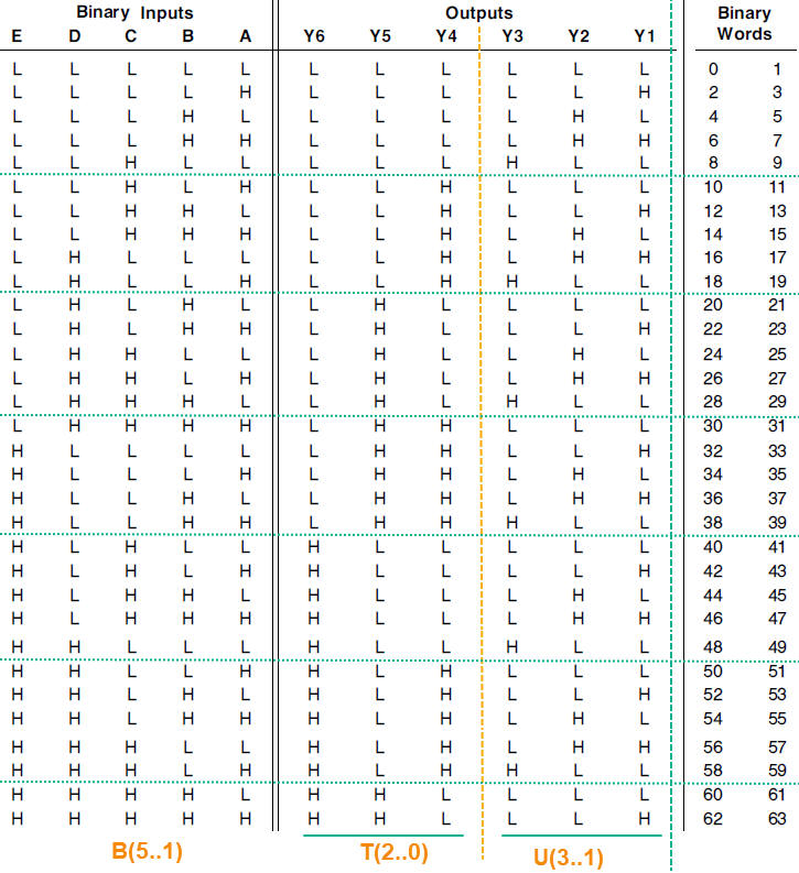
Fig. 2. Bin_BCD_6bit component truth table. Adapted from the DM74185 datasheet. This chip is capable of converting any 6-bit radix-2 number into BCD (from 0 to 63). |
Draw the sketch of a timing diagram to demonstrate how the circuit works for several input stimulus.
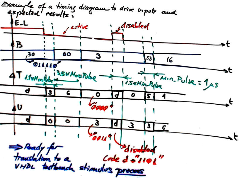 |
| Fig. 3. Example timing diagram. |
Using BCD_7seg_decoder chips we can display the BCD numbers as represented in Fig. 4.
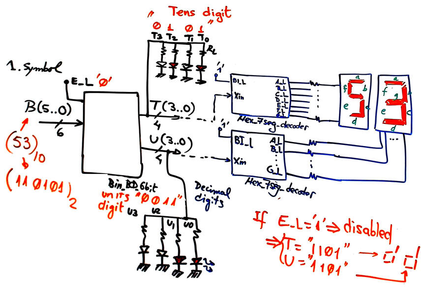 |
| Fig. 4. Application to represented the BCD numbers in 7-segment displays. |
This is the article from Wikipedia: the double dabble algorithm is used to convert radix-2 numbers into BCD.
2. Planning
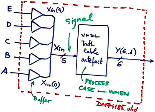
Draw an schematic to be able to use the truth table artefact.
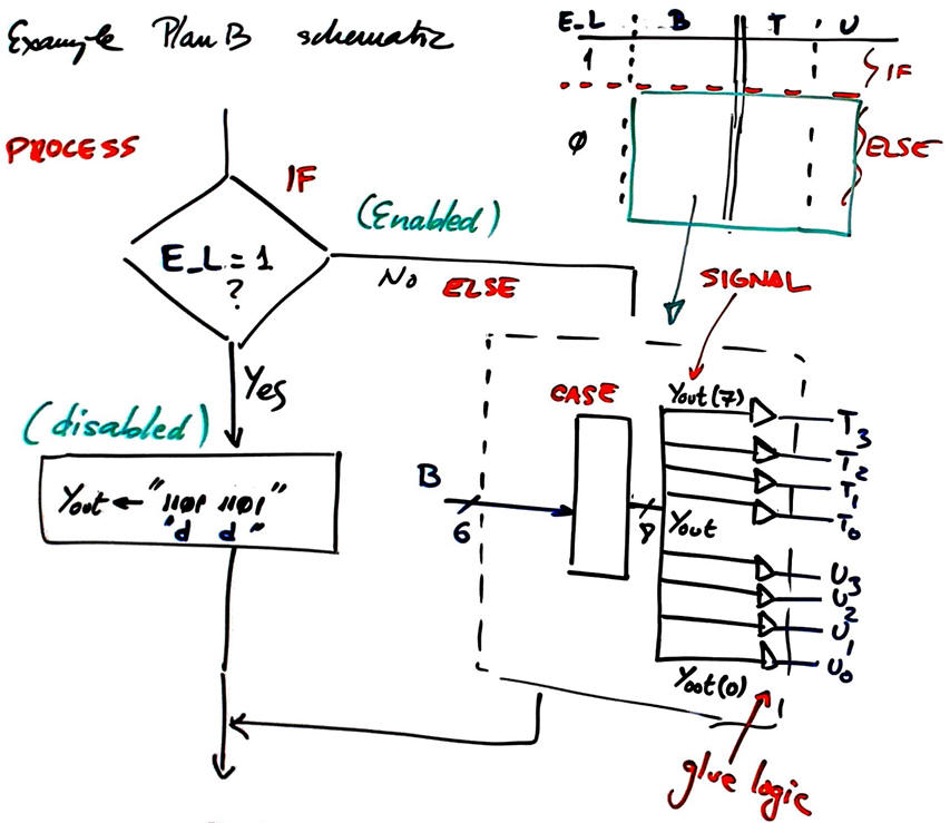 |
| Fig. 5. High-level schematic ready for VHDL translation. |
Project and file locations:
C:\CSD\P2\Bin_BCD_6bitB/(files)
3. Development
Find a similar VHDL description for a plan B circuit, copy and adapt. This is the schematic in Fig. 5: Bin_BCD_6bit.vhd
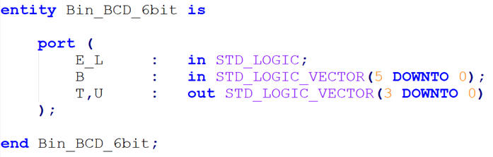 |
| Fig. 6. Entity definition is the same whatever the plan. |
Start an EDA synthesis project named Bin_BCD_6bit_prj for a given target chip, for example Intel CPLD EPM2210F324C3 and examine results.
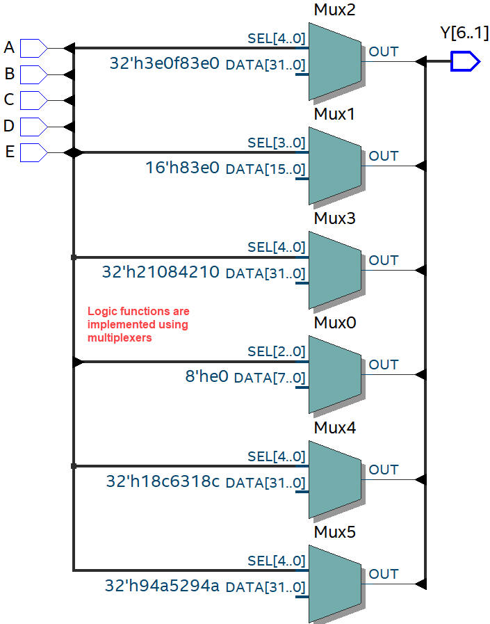
Fig. 7. RTL schematic of the Bin_BCD_6bit using high-level description. |
Technology view schematic.
|
Fig. 8. Technology view of Bin_BCD_6bit targeting Intel CPLD: EPM2210F324C3. The Chip Planner tool in Quartus Prime can be used to locate exactly where your circuit is synthesised in the CPLD lattice of logic cells. |
4. Testing
In Fig. 9 is represented the testbench schematic to stimulate the unit under test (UUT) with input vectors. In a step #1 generate the skeleton of the testbench file, in a step #2 add stimulus translating to VHDL input activity from the time diagram in Fig. 3. This is an example of a simple test bench Bin_BCD_6bit_tb.vhd from which you can copy the constant Min_Pulse and the stimulus process.
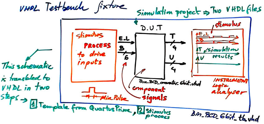 |
| Fig. 9. Testbench fixture to verify that our circuit works as expected. |
Start the VHDL simulator project, Bin_BCD_6bit_functional_sim, and run the test. Verify applying sufficient test vector that the device works as expected (verify how the information of each channel is selected). Print timing diagram screen and add comments on the signals to show how the device works.
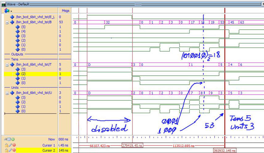 |
| Fig. 10. Ideal functional simulation waveform results from the logic analyser. |
5. Report
6. Prototyping
1.- Specifications
Design the DM74185 chip functionality to be used as building block for larger binary to BCD converters as shown in the datasheet. This block is an optimisation of the double dabble algorithm for translating numbers from radix-2 to BCD.
The symbol and the way it converts 6-bit numbers from radix-2 into BCD is represented in Fig. 1. Six output functions to represent tens and units digits when including input B(0).
  |
| Fig. 1. DM74185 symbol and edited truth table from the datasheet. |
2.- Planning
We organise the behavioural schematic (plan B) in Fig. 2 to adapt the VHDL truth table process artefact to inputs and outputs.
 |
| Fig. 2. High-level schematic for capturing directly the truth table in a single step. |
3.- Development
This DM74185.vhd is the translation of the behavioural schematic in Fig. 2.
 |
| Fig. 3. RTL view from the high-level VHDL truth table translation. |
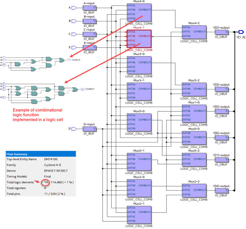 |
| Fig. 4. Technology view. 14 logic elements are used to implement this block. |
4.- Test
We can drive the circuit with some input vectors and check the outputs Y(6..1). This is an example of testbench translation to VHDL DM74185_tb.vhd.
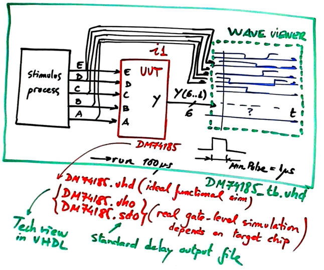 |
Fig. 5. Testbench organisation. We can use the same testbench for functional and gate-level simulations. |
Fig. 6 shows results from a functional simulation.
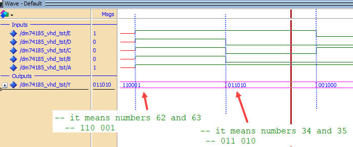 |
Fig. 6. Results accordingly to the truth table. |
| Home Term 26/27-Q1 Contact Products Electronic devices and companies Software Books Magazines Instruments DEE Library EETAC DEEL |

|
|
| Web activa des de 09/2001, @ F. J. Robert, Web editat amb Microsoft Expression Web 4. El contingut és un complement als materials d'estudi del curs Circuits i Sistemes Digitals disponibles al campus digital Atenea. Llicència:Reconeixement 4.0 Internacional de Creative Commons |