|
|
Bachelor's Degree in Telecommunications Systems and in Network Engineering |
|
|
DE10-Lite board: setup, verification and examples |
||
| 1. Terasic DE10-Lite board | 2. FPGA | 3. USB driver | 4. Example |
Terasic DE10-board
We can implement prototypes for simple circuits using academic boards such Terasic DE10-Lite populated with an Intel MAX10 FPGA. This is the 6th step in our VHDL design flow that includes project management, VHDL source files editing, circuit synthesis and simulation, and chip programming.
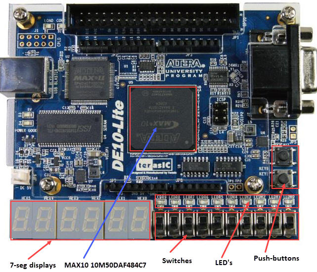 |
| Fig. 1. DE10-Lite board, user manual and drivers at Terasic. |
Before using the board we have to install the drivers and check that cables and connections are all right. In this unit we explain these steps including an example circuit design: a 2-digit binary to 7-segment decoder.
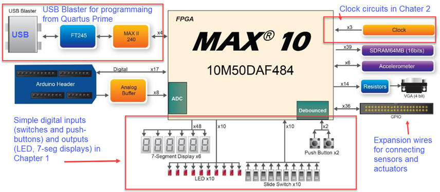 |
| Fig. 2. In CSD we will use only a reduced set of features from DE10-Lite board, basically simple digital inputs and outputs. In chapter 2 we will include as well clocked synchronous circuits. |
| 1. Board | 2. FPGA | 3. USB driver | 4. Example |
2. Programmable logic device (PLD), field programmable gate array (FPGA) Intel MAX10
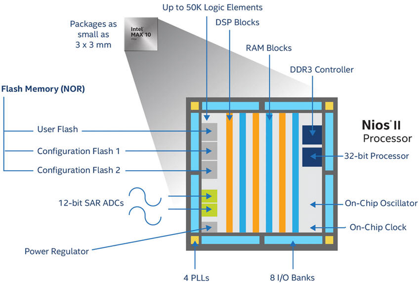
MAX 10 device 10M50DAF484C7 containing up to 50k programmable logic elements is placed in DE10-Lite board. Technology details and datasheets can be studied at Intel page. Additional basic concepts on programmable logic devices can be read in this unit PLD.
 |
| Fig. 3. 10M50DAF484C7 FPGA (ref.) |
We will use this chip at its basic level, paying attention only to its logic elements (LE) capable of implementing logic functions using the plan of RAM memories with 4-input granularity. The chip contains 50.000 of them, meaning that all our introductory projects will fit easily in a single FPGA.
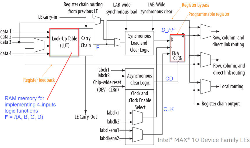 |
| Fig. 4. Logic element structure. In Chapter 2 we will use as well the synchronous 1-bit memory cell D_FF. |
| 1. Board | 2. FPGA | 3. USB blaster driver | 4. Example |
Windows 11 USB Blaster driver
The first step when experimenting with prototypes is to validate the board. This includes installing its Windows driver and downloading the default configuration as if we had just acquired the board.
Download from Terasic and unzip the DE10-Lite system CD where to find manuals, drivers and schematics. Note: You can find it as well in our Google Drive shared folder.
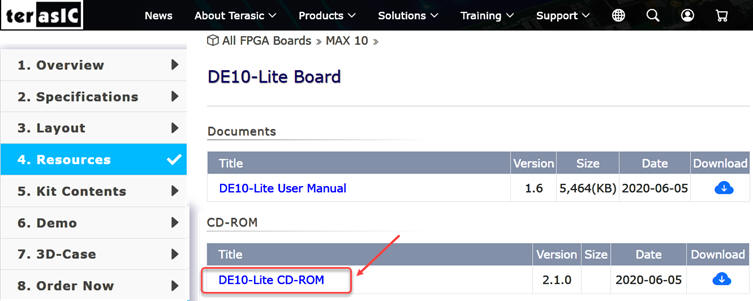 |
| Fig. 5. Resources for the board De10-Lite. |
Windows 11 generates complications with the USB Blaster driver for this board, because it is not signed and the operating system do not allow its installation as usual. From this Terasic forum, you find instructions on how to proceed with the USB driver installation to interface the DE10-Lite board. This contribution from CSD students will help you to solve this issue on unsigned drivers.
 |
Fig. 6. The unsigned version of the USB Driver is found in this forum. USB Blaster Driver From Q16.1. Unzip it into a known location, for instance: "C:\tmp\Usb_blaster_q16.1". More information here. |
Open the Windows 11 Control Panel. Select "Hardware and sound", "Device Manager" and proceed as follows to nstall the USB Blaster as follows:
 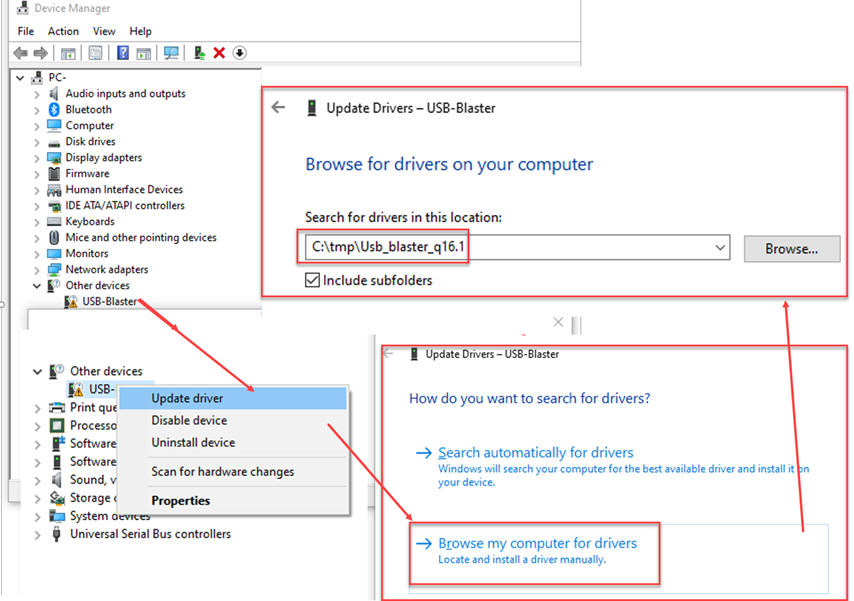 |
| Fig. 7. Find the driver file and install it. |
Fig. 8 shows the installation process that finishes when the DE10-Lite board is correctly identified as another fully operational USB device connected to the PC.
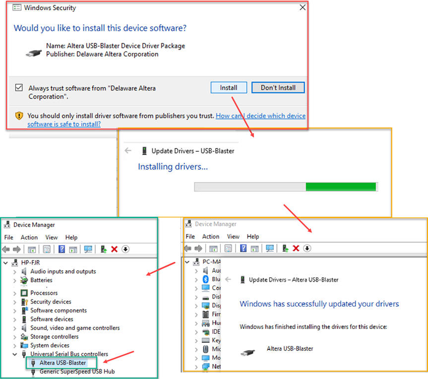 |
| Fig. 8. Completing the driver installation. |
Finally, to validate the driver installation and the board, downloading the default configuration "DE10_LITE_Default.pof" as if we had just acquired the board. As shown in Fig. 9, you can open the programmer from its logo in Quartus Prime or as an standard alone application:
 |
Fig. 9. Accessing the Programmer. |
"Add file" to the programmer and be aware that the USB-Blaster is recognized by the system and the hardware interface.
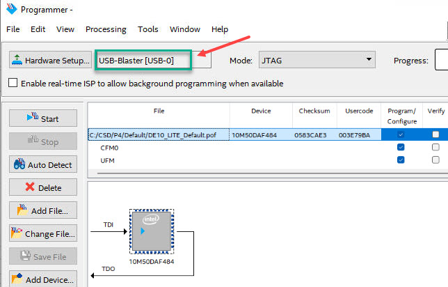 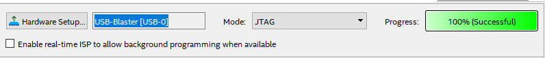 |
| Fig. 10. Programming the default configuration to validate the driver and the board. |
(Optional) Control Panel default application
Once the USB-Blaster driver installed, if the computer already has been using Quartus Prime, we can control the DE10-Lite board resources from the Control Panel application found in the CD disk from Terasic. Let us test the switches, LED and 7-segment displays.
Firstly, as seen in Fig. 11, from the directory System CD --> Tools --> ControlPanel, copy the "bin" library to where Quartus Prime is installed in your PC, for example at C:\intelFPGA_lite\20.1\quartus
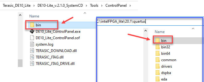 |
Fig. 11. Copying the ControPanel "bin" library to Quartus Prime folders. |
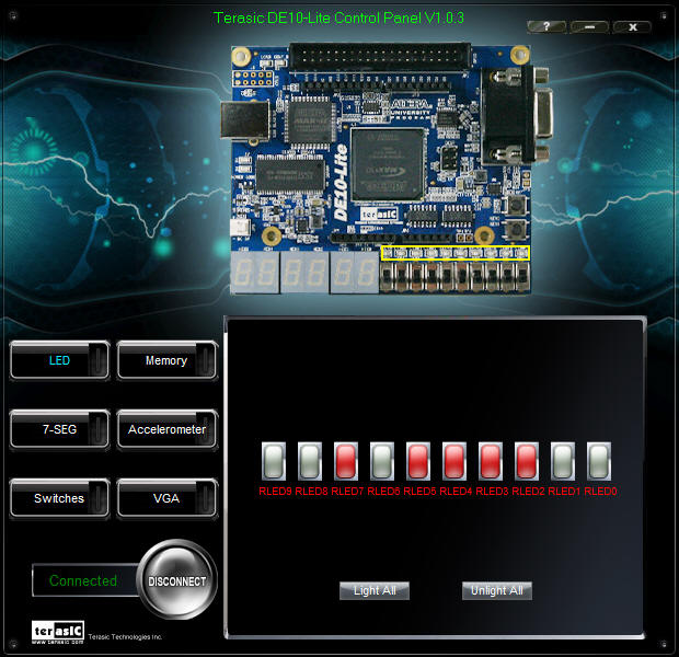
And secondly, as shown in Fig. 12, run the "ControlPanel.exe" application to visualise buttons, switches, LED and 7-segment display digits.
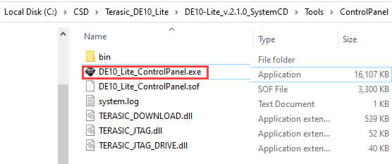 |
Fig. 12. Control panel application for verifying the cable and the De10-Lite interface to the PC. |
 |
|
Once the hardware and software is working correctly in our computer, we can start experimenting. The next section below shows a complete combinational circuit prototype example, as you will see in other CSD designs.
| 1. Board | 2. FPGA | 3. USB driver | 4. Example |
Let us program the MAX10 chip in the DE10-Lite board with a given project.
| Prototype specifications | Planning | Development | Test & measurements |
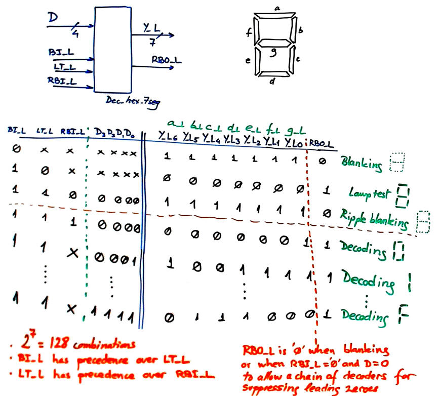
Using the HEX_7SEG_decoder invented in P2 applying plan A (or the same Hex_7seg_decoder applying plan B), design a new chip Dec_hex_7seg that includes active-low ripple blanking input (RBI_L) and output (RBO_L) for cascadable zero-suppression capability (this is blanking leading zeroes), and also lamp test (LT_L) functions. This means completing the functionality of the standard 74LS47 chip applying plan C2.
 |
 |
| Fig. 1. Dec_hex_7seg symbol and truth table. Example of timing diagram. |
Try in our Proteus virtual laboratory how a chain of several decoders can be implemented for blanking or suppressing leading zeroes in this Hex_7seg_decoder.pdsprj using such control signals as ripple blanking input and output.
| Prototype specifications | Planning | Development | Test & measurements |
As represented in Fig. 2, we will use plan C2 connecting Chip1 and extra logic for implementing the blanking and lamp test functionality.
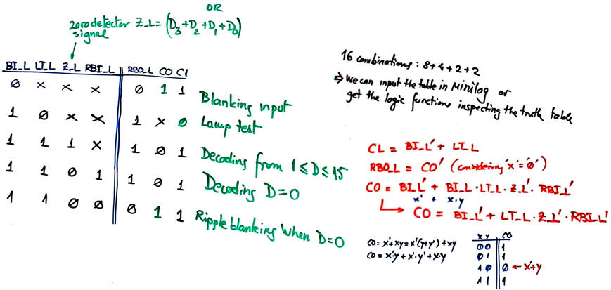 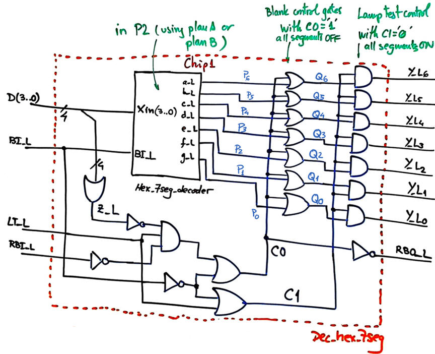 |
| Fig. 2. Proposed plan C2 circuit. The additional logic will complete the specifications solved by Chip1. |
Project location:
C:\CSD\P3\Dec_hex_7seg\(files)
| Prototype specifications | Planning | Development | Test & measurements |
Let us translate our plan above in Fig. 2 to VHDL: "Dec_hex_7seg.vhd", and start a new Quartus Prime synthesis project targeting specifically the FPGA 10M50DAF484C7 populating the DE10-Lite board. Include in this project a copy of the component Hex_7seg_decoder from P2 (plan A or plan B).
Once the circuit is synthesised we obtain the ideal or register transfer level (RTL) schematic as shown in Fig. 3.
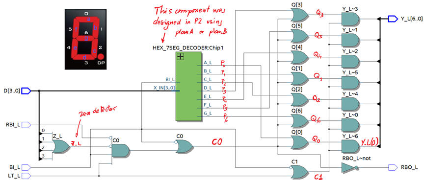 |
| Fig. 3. RTL view. |
In this project we use 18 logic elements to implement the eight output functions in this 128 row truth table.
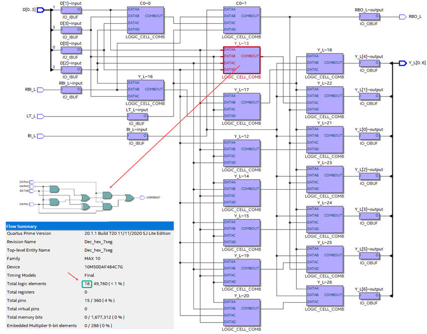 |
| Fig. 4. Technology schematic. |
| Prototype specifications | Planning | Development | Test & measurements |
1. Functional simulation
Let us imagine the test bench as usual as represented on Fig. 5. Generate the template from Quartus Prime.
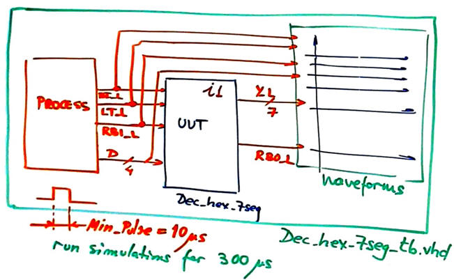 |
Fig. 5. Testbench fixture to verity our design. |
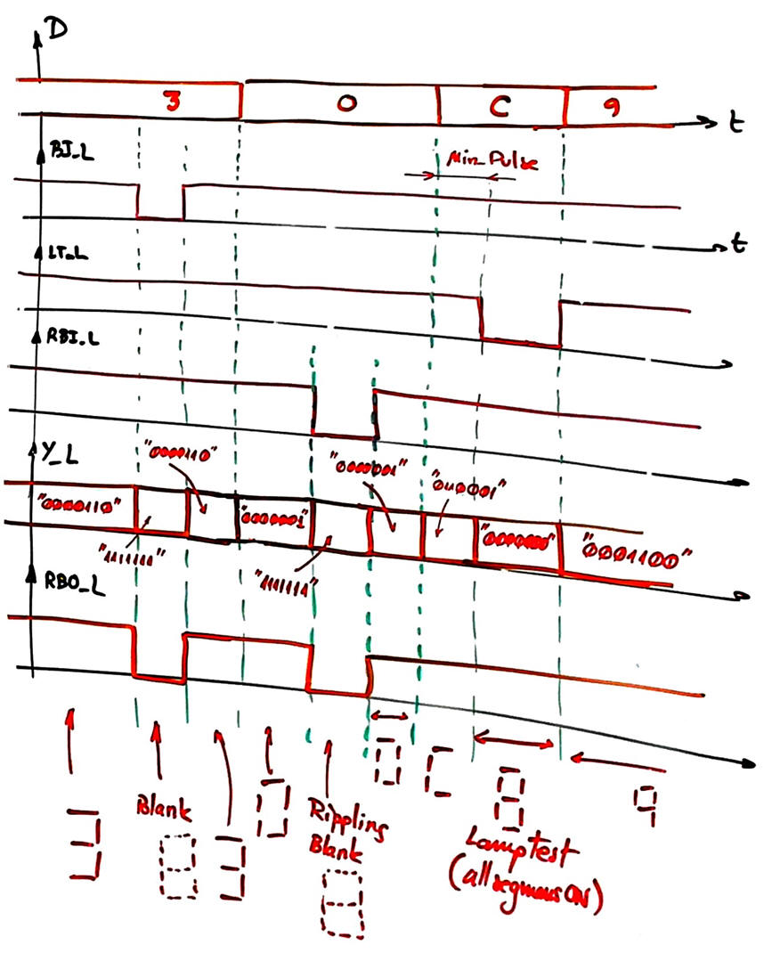
Translate the stimulus as in this example file "Dec_hex_7seg_tb.vhd" and set for instance Min_Pulse = 10 µs and run the ModelSim simulation for 300 µs.
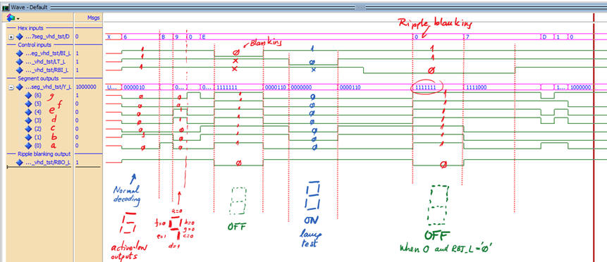 |
| Fig. 6. Functional simulation results. |
NOTE: Unfortunately, MAX10 technology does not generate standard delay output files (sdo), making impossible running real gate-level simulations in ModelSim. However, we can still use the Quartus Prime timing analyser tool to measure propagation delays.
2. Board configuration and pin assignments
We have to read the DE10-Lite user manual to find which pins are used for LED, switches and seven segment displays.
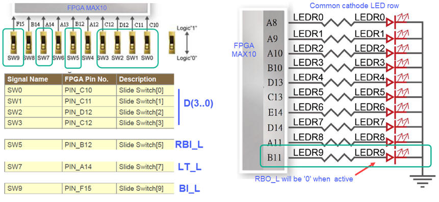 |
| Fig. 7. Pins assigned to the LED row. We propose to use LED9 for representing RBO_L output. We also can used six of the 8 switches available for D(3..0) and BI_L, LT_L and RBI_L inputs. |
We can use one of the six available 7-segment displays to represent decoded hexadecimal symbols. For instance, HEX3 as shown in Fig. 8.
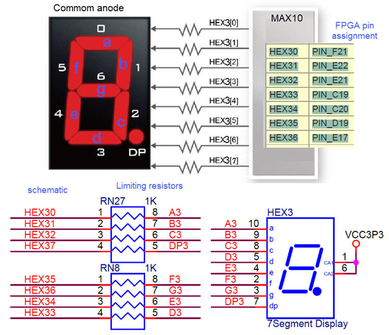 |
| Fig. 8. Circuitry associated to 7-segment displays from the user manual and the schematics from Terasic. LED segments are using a 1 kΩ limiting resistors for biasing at IDQ = 1.8 mA. |
Let us run the pin planner spreadsheet tool from Quartus Prime as shown in Fig. 9 to annotate inputs and output pins.
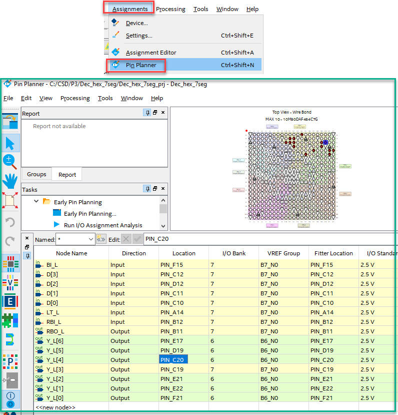 |
| Fig. 9. Pin assignment tool. |
Pin listing can be exported and imported in spreadsheet format (."csv" extension) Dec_hex_7seg_prj_pins.csv, making it simple continuing projects and adding new features to existing ones.
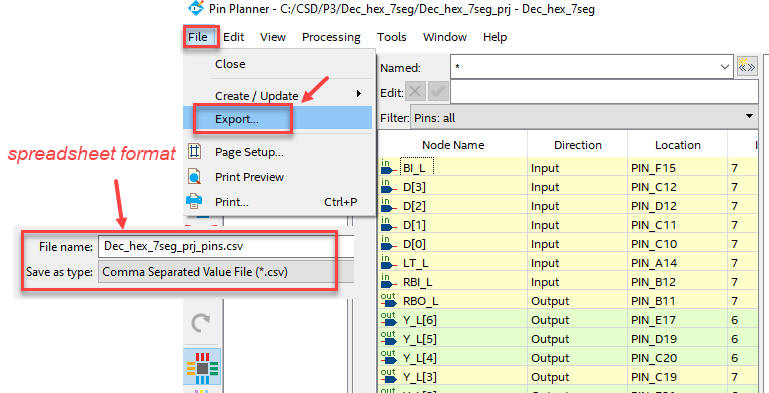 |
| Fig. 10a. Exporting the list of pins from Pin Planner and saving it as "*_pins.csv" in project directory.
|
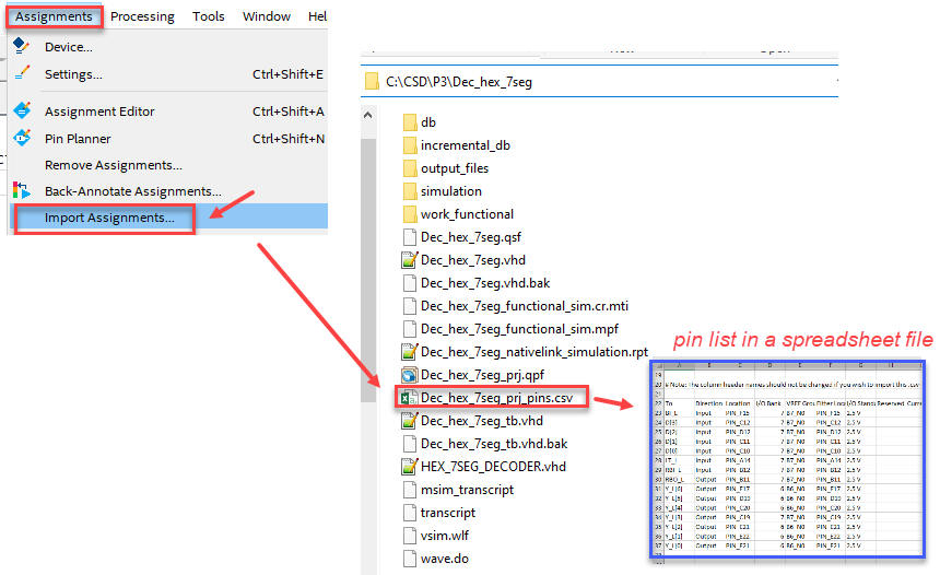 |
| Fig. 10b. Importing from Quartus Prime the list of pin assignments. |
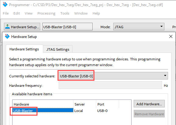
Synthesise all and finally run the programmer selecting the icon from Quartus Prime top tap as shown in Fig. 11. Select the USB-Blaster as the default programming hardware. It has to be identified correctly if the DE10-lite driver were successfully installed in Fig. 8 above.
 |
| Fig. 11. USB-Blaster has to be detected and assigned to the programmer tool. |
Assign the output SOF file Dec_hex_7seg.sof to the MAX10 chip and click start programming. In a few seconds the device will be ready to use.
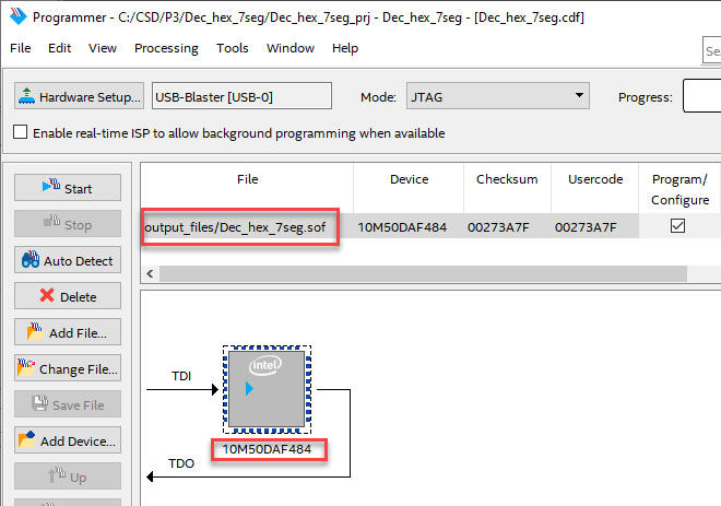 |
| Fig. 12. Select the SOF file located at: "C:\CSD\P3\Dec_hex_7seg\output_files", and click "Start". |
DE10-Lite board must work as pictured in Fig. 13. You can try inputs and check the circuit truth table.
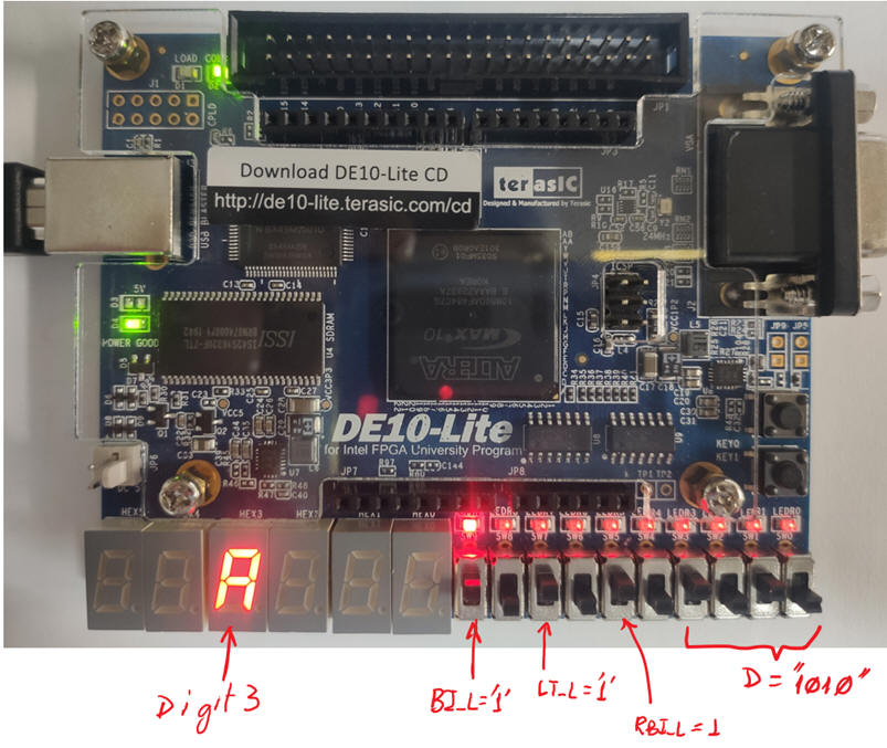 |
| Fig. 13. Picture of the final prototype running our project Dec_hex_7seg. |
This is the full (zipped) list of VHDL files for this new project "Dec_hex_7seg.zip" in Fig. 2.
Note: In case we like to write the configuration flash memory (CFM) of the FPGA and make the circuit permanent (not erased when unplugging the board), the programmer object file (.pof) is required: "Dec_hex_7seg.pof".
Note: You can modify your symbol and assign to all unused LED outputs a '0' to switch them all off.
Note: : This is the board's default application in case you like to restore it: "DE10_LITE_Default.pof", copied from the board's system CD-ROM.
| 1. href="#top">Board | 2. FPGA | 3. USB driver | 4. Example | 5. GPIO Expansion |
GPIO expansion board
We can add many more inputs or outputs to the DE10-Lite board connecting expansion boards through the 40-pin cable. Such experiments are proposed in LAB4.2 (ALU_9bit), and also in LAB2 (MUX_DeMUX).
| Home Term 26/27-Q1 Contact Products Electronic devices and companies Software Books Magazines Instruments DEE Library EETAC DEEL |

|
|
| Web activa des de 09/2001, @ F. J. Robert, Web editat amb Microsoft Expression Web 4. El contingut és un complement als materials d'estudi del curs Circuits i Sistemes Digitals disponibles al campus digital Atenea. Llicència:Reconeixement 4.0 Internacional de Creative Commons |