|
|
Bachelor's Degree in Telecommunications Systems and in Network Engineering |
|
|
|
||
|
|
Int_Mult_9bit plan C2: hierarchical multiple-file VHDL |
|
|
|
||
1. Specifications
Design a multiplier for 9-bit integer numbers. Use plan C2 and include the Mult_9bit block for radix-2 binary numbers as the main component.
Fig. 1. Symbol, truth table and an example of timing diagram of what is expected from this circuit. |
The positive value of the multiplication Q(17..0), its absolute value is also available, ready to be used for representing the result in BCD 7-segment displays.
This is an example in Proteus on how an 8-bit radix-2 multiplier Mult_8bit.pdsprj works.
This is a Selectable_mult_8bit.pdsprj in Proteus on how to use an 8-bit multiplier Mult_8bit for two types of numbers: (1) integers in two's complement and (2) radix-2.
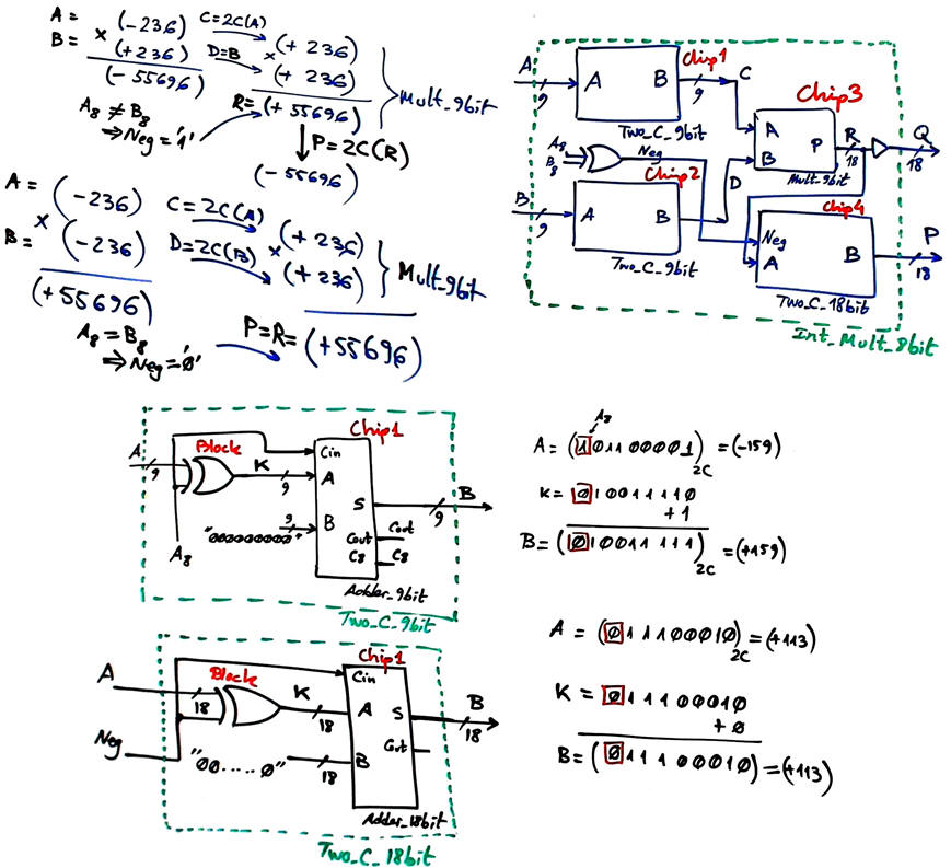
2. Planning
The idea is to use a radix-2 multiplier Mult_9bit also as the basic component for integer multiplications. Thus, the sign bit will indicate when to generate two's complements of the operands or the result.
 |
|
Fig. 2. Idea of signed multiplications. |
Project folder:
C:/CSD/P4/Int_Mult_9bit/(files)
Translate the circuit in Fig. 2 to VHDL as usual: Int_Mult_9bit.vhd.
The key component Chip3 for multiplying 9-bit wide radix-2 numbers is in this tutorial: Mult_9bit.
These are the arithmetic blocks: Adder_18bit.vhd, Adder_1bit.vhd, Adder_4bit.vhd, Adder_9bit.vhd, Carry_generator.vhd, Two_C_18bit.vhd, Two_C_9bit.vhd.
|
Fig. 3. RTL. |
|
Fig. 4.Technology |
4. Testing (functional simulation)
The testbench fixture containing the main ideas and concepts involved in this schematic is represented in Fig. 7.
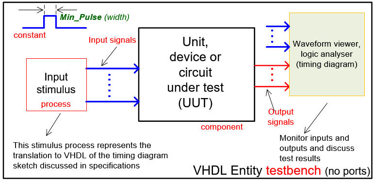 |
Fig. 5. Testbench VHDL schematic. |
Convert the initial timing diagram sketch into a VHDL testbench like in this file Int_Mult_9bit_tb.vhd writing input activity process and Min_Pulse constant in the template produced by the EDA tool. Use positive and negative numbers as inputs to the circuit.
Run the EDA VHDL simulator and demonstrate how the circuit works adding comments to the printed sheet of paper containing the waveforms.
|
|
Fig. 6. Example test with some input vectors A, B. |
5. Testing (gate-level simulation)
VHDL design flow shows how gate-level simulations represent the 5th design step. Run a gate-level simulation to measure the propagation delay in a given transition.
|
|
Fig. 7. Example waveform for the Int_Mult_9bit showing how a given input vector is computed over time generating wrong results until all signals have propagated through the circuit. In this transition it takes 10 ns to obtain the correct result. |
Use the timing analyser tool to determine worst-case scenario, and thus the maximum speed of comparison operations. In this example, the comparator can handle xxx millions of comparisons per second.
|
|
Fig. 8. Timing analyser spreadsheet. For a target chip MAX II the longest propagation time is tP = xxx ns. |
Repeat measurements for Intel Cyclone IV, and compare results.
Perform a simulation to show that the circuit cannot produce correct results when the Min_Pulse constant is less that the worst case (longest) delay.
6. Report
Follow this rubric for writing reports.
7. Prototyping
A prototype for the DE10-Lite board that used this component to perform integer multiplications is the ALU_9bit in Lab4.
| Home Term 26/27-Q1 Contact Products Electronic devices and companies Software Books Magazines Instruments DEE Library EETAC DEEL |

|
|
| Web activa des de 09/2001, @ F. J. Robert, Web editat amb Microsoft Expression Web 4. El contingut és un complement als materials d'estudi del curs Circuits i Sistemes Digitals disponibles al campus digital Atenea. Llicència:Reconeixement 4.0 Internacional de Creative Commons |