|
|
Bachelor's Degree in Telecommunications Systems and in Network Engineering |
|
|
|
||
|
|
HEX_7seg_decoder plan B: behavioural single-file VHDL (flat) |
|
|
|
||
Hexadecimal to 7-segment decoder (type 74LS47)
| 1. Specifications | Planning | Developing | Testing | Report | Prototype |
Design a HEX_to_7SEG decoder using plan B, behavioural description of the specifications , i. e. the truth table. This is the circuit's symbol, truth table, and timing diagram.
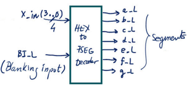 |
| Fig. 1. Hexadecimal to 7-segment decoder. A similar standard chip is the 74LS47. |
When BI_L is active with a low level ('0'), all outputs are high ('1'), meaning that no LED is lighting (blanked).
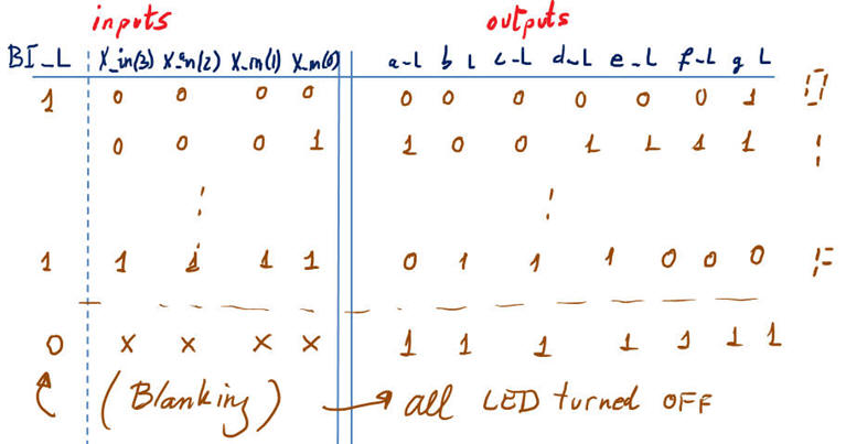 |
| Fig. 2. This is the truth table to define how the circuit works and that always goes attached to the symbol. |
Example of a timing diagram. Plan some input vectors and figure out which are going to be the outputs.
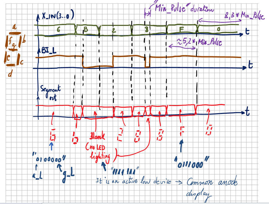 |
| Fig. 3. The sketch of the timing diagram that is expected from this circuit. |
Fig. 4 represents a similar circuit Dec_hex_7seg.pdsprj with additional control signals captured for running in Proteus simulator.
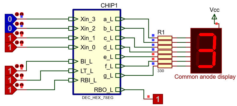 |
| Fig. 4. A hexadecimal to 7-segment decoder in Proteus. This chip has three additional active-low control inputs and outputs: ripple blanking input (RBI_L), ripple blanking output (RBO_L) and lamp test (LT_L), as defined in standard chip 74LS47. |
The same project Hex_7seg_decoder using plan A, thus you can compare both internal architectures.
| Specifications | 2. Planning | Developing | Testing | Report | Prototype |
1. This is our VHDL design flowchart for transferring circuit specifications into a digital circuit realisation targeting CPLD or FPGA chips.
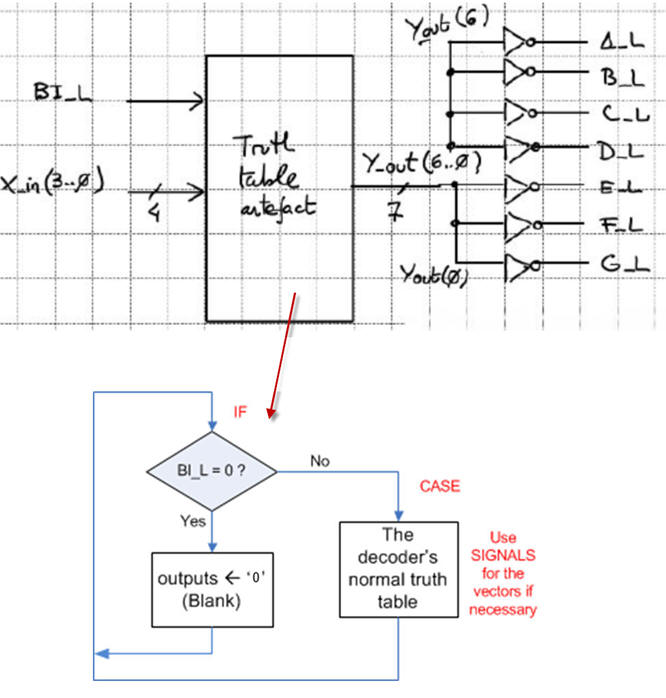
2. Study how to organise a schematic of a circuit in VHDL to translate the complete truth table construct with input and output ports and signals. Fig. 5 shows an example where you can mix a flowchart and and schematic with ports and vector inputs and outputs.
 |
|
Fig. 5. This is the schematic that represents the truth table, ready to be translated to VHDL (as shown below in the development section). |
3.- Run a EDA tool project for a CPLD/FPGA chip (hex_7seg_decoder_prj) and print the RTL view.
4.- Test the project using a VHDL testbench (and for instance the stimulus timing diagram represented above in Fig. 3).
| Specifications | Planning | 3. Developing | Testing | Report | Prototype |
1.- Write down a VHDL file (hex_7seg_decoder.vhd ) which contains an architecture of the circuit based on a behavioural description, for example the schematic in Fig. 5. This behavioural interpretation of the truth table looks somewhat like a computer algorithm, but is a circuit (hardware).
2.- Start an EDA tool project for a CPLD/FPGA chip (hex_7seg_decoder_prj) and obtain the synthesised circuit. Represent and analyse the RTL and technology views.
This below in Fig. 6 is an example of RTL schematic of the circuit synthesised by the computer tool. In this case, because we have not described a given structure based on equations, but the truth table itself, the synthesiser decides what is best.
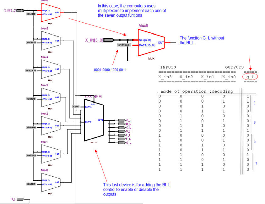 |
| Fig. 6. Example of RTL view. |
| Specifications | Planning | Developing | 4. Testing | Report | Prototype |
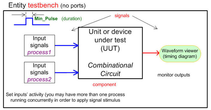
1.- Start an EDA VHDL simulator project and verify the Device-Under-Test (DUT) using a VHDL simulator test bench (HEX_7SEG_decoder_tb.vhd).
 |
|
Fig. 7. This is the testbech idea schematic that you can adapt to your problem. for example adding the stimulus represented in the timing diagram from the project specifications in Fig. 3. |
2.- Verify applying sufficient test vector that the device works as expected (verify the truth table). Print timing diagram screen and add comments on the signals to show how the device works.
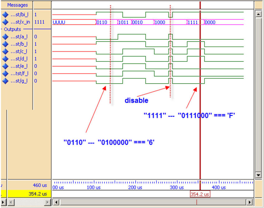 |
| Fig. 8 This is an example of functional simulation of the Unit Under Test (UUT). |
| Specifications | Planning | Developing | Testing | 5. Report | Prototype |
Follow this rubric for writing reports.
| Specifications | Planning | Developing | Testing | Report | 6. Prototype |
We can use the DE10-Lite board to implement this project, as shown in DE10-Lite tutorial unit. Study the user manual and generate a HEX_7seg_decoder_top schematic to assign input and output pins.
| Home Term 26/27-Q1 Contact Products Electronic devices and companies Software Books Magazines Instruments DEE Library EETAC DEEL |

|
|
| Web activa des de 09/2001, @ F. J. Robert, Web editat amb Microsoft Expression Web 4. El contingut és un complement als materials d'estudi del curs Circuits i Sistemes Digitals disponibles al campus digital Atenea. Llicència:Reconeixement 4.0 Internacional de Creative Commons |