|
|
Bachelor's Degree in Telecommunications Systems and in Network Engineering |
|
|
|
Adder_16bit plan C2: carry-lookahead (CLA) |
16-bit adder for radix-2 numbers
| 1. Specifications | Planning | Developing | Functional test | Gate-level test | Prototype | Report |
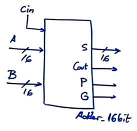
Design an Adder_16bit using the carry-lookahead (CLA) technique. The additional signals in this symbol P (propagator) and G (generator) are outputs required for chaining larger adders using the same CLA architecture.
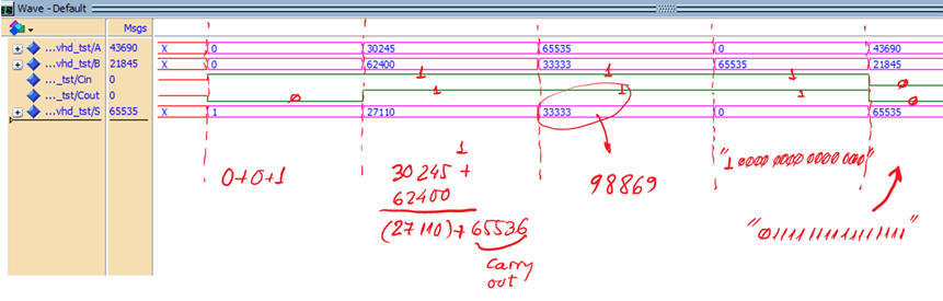
The truth table and timing diagram are the same stated in Adder_4bit CLA considering now radix-2 operands A and B ranging from 0 up to 65535 = "1111 1111 1111 1111".
 |
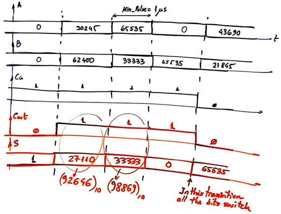 |
| Fig. 1. Symbol and waveforms. |
|
Here we rely on the work done when designing the tutorial Adder_4bit CLA. For instance, read in Wikipedia how an Adder_16bit works and how it is possible to calculate all carries beforehand. This reference also explains how to chain carry generators: Ercegovac, M., Lang, T., Moreno, J. H., "Introduction to Digital Systems", John Wiley & Sons, 1999). It includes slides: Chapter 10 is on arithmetic circuits.
| Specifications | 2. Planning | Developing | Functional test | Gate-level test | Prototype | Report |
Fig. 2 shows the picture from Wikipedia that is adapted in CSD as Fig 3.
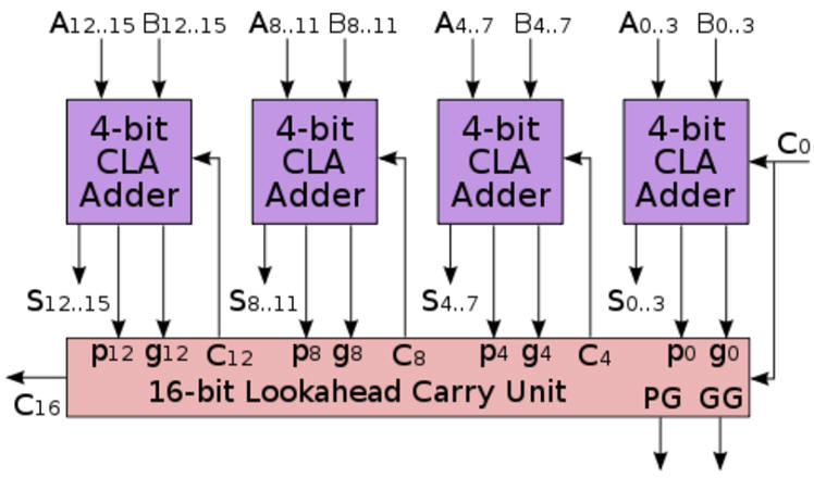 |
| Fig. 2. Adder_16bit architecture proposed in Wikipedia to be written in CSD as VHDL file. |
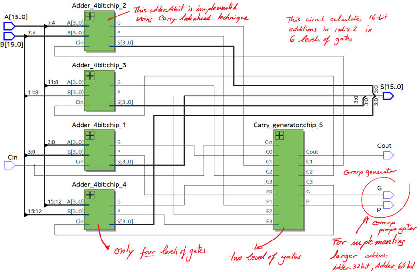
The Adder_16bit has the same structure than the circuit designed in Adder_4bit, as shown in Fig. 3.
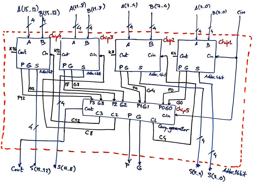 |
| Fig. 3. Planning the Adder_16bit. A schematic totally annotated ready to be transferred into VHDL. |
What is the number of gate levels (NGL) expected in this circuit?
Project location:
C:\CSD\P4\Adder_16bit_CLA\(files)
| Specifications | Planning | 3. Developing | Functional test | Gate-level test | Prototype | Report |
We will pick up the same Intel MAX II EPM2210F324C3 target chip. Thus, the same chip will implement the same entity but with two alternative architectures.
This is the VHDL file translation of the architecture in Fig. 3: "Adder_16bit.vhd".
Components "Carry_generator.vhd" and "Adder_4bit.vhd" can be found in tutorial Adder_4bit.
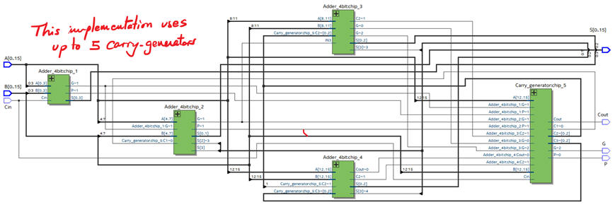
Start a VHDL synthesis project and observe the schematics in the RTL view. This time the architecture is far more complex, compromising up to 71 logic elements; more chip logic resources with the aim of obtaining a faster circuit.
 |
| Fig. 4. RTL view. |
The architecture uses up to five Carry_generator circuits organised in two levels (one Carry_generator in each Adder_4bit module, and another one in the top entity). However, NGL = 6.
 |
| Fig. 5. Technology view. |
The Quartus Prime Chip Planner tool allows us to map exactly where all the resources in use are located.
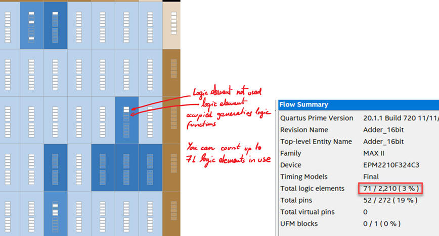 |
| Fig. 6. MAX II chip occupation from chip planner tool. |
| Specifications | Planning | Developing | 4. Functional test | Gate-level test | Prototype | Report |
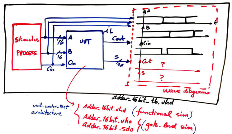
Now, it is time to test the synthesised circuit above. Thus, we can use the same VHDL fixture represented in the Fig. 5 of the previous project Adder_16bit RC.
Example of testbench "Adder_16bit_tb.vhd" from which to copy the stimulus signals and the constant Min_pulse. We are expecting the same ideal functional results represented in Fig. 7 when applying the same input vectors.
 |
| Fig. 7. Functional results. |
| Specifications | Planning | Developing | Functional test | 5. Gate-level test | Prototype | Report |
Now, when running a gate-level simulation at the same transition, a shorter propagation delay is obtained. Only 12.6 ns (saving 10 ns from the same design above based on ripple-carry).
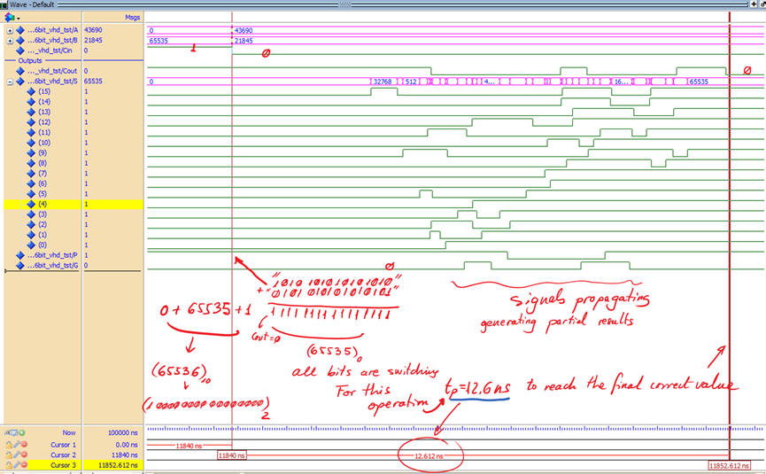 |
| Fig. 8. Gate-level simulation. |
And, finally, measuring the longest propagation delay using the timer analyser tool, we can deduce the maximum circuit's speed. The longest signal path is established between input A(6) and output S(11), tP = 14.3 ns. This circuit is capable of a theoretical maximum of speed = 70 Mops. Thus, an improved architecture using more hardware (logic elements) generates a faster circuit.
The drawback is that the dynamic power consumption will be higher than the same circuit based on the RC technique. At this CSD introductory level, and from the perspective of classic technologies, we can say that the static power consumption will be larger because there are more gates connected to the power supply, and the dynamic power consumption will also be larger because there are many more logic gates switching.
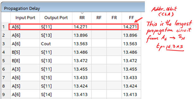 |
| Fig. 9. Timing analyser spreadsheet showing CLA adder results. |
| Specifications | Planning | Developing | Functional test | Gate-level test | 6. Prototype | Report |
| Specifications | Planning | Developing | Functional test | Gate-level test | Prototype | 7. Report |
Follow this rubric for writing reports.
| Home Term 26/27-Q1 Contact Products Electronic devices and companies Software Books Magazines Instruments DEE Library EETAC DEEL |

|
|
| Web activa des de 09/2001, @ F. J. Robert, Web editat amb Microsoft Expression Web 4. El contingut és un complement als materials d'estudi del curs Circuits i Sistemes Digitals disponibles al campus digital Atenea. Llicència:Reconeixement 4.0 Internacional de Creative Commons |