|
|
Bachelor's Degree in Telecommunications Systems and in Network Engineering |
|
Push-button circuits. (A) debouncing filter, (B) synchroniser |
| 1. Specifications | Planning | Developing | Testing (functional) | Testing (gate-level) | Prototype | Report |
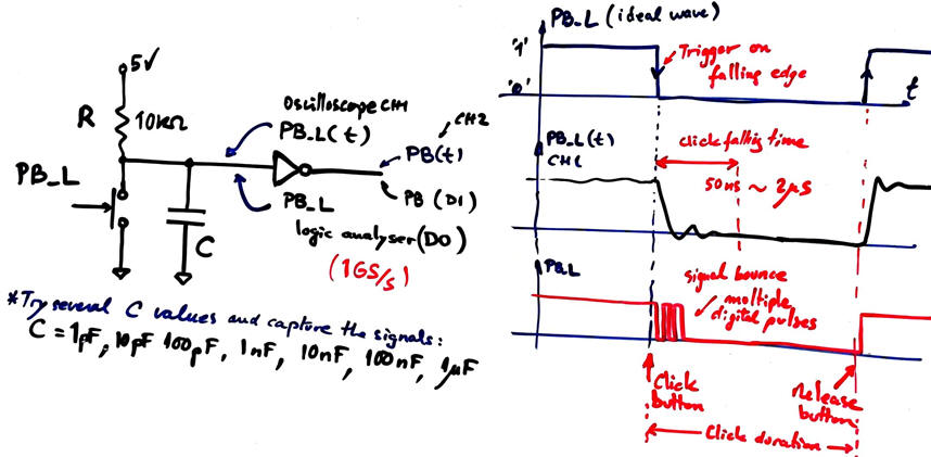
Let us design a digital filter to clean the noisy signal generated when pressing and releasing a mechanical key or pushbutton. When clicking and releasing a key, the electrical signal generates a random number of ones and zeros (signal bouncing) that must be filtered out in order to interface correctly a digital circuit. Additionally, the idea is to synchronise the key signal (an asynchronous input) to the system CLK, so that it can be correctly sampled. This phenomena is sampled correctly in the range of 100 Hz.
 |
Fig. 1. Example of the waveforms describing the phenomena. Clicking a mechanical key has to generate a clean single pulse (visio). |
Thus, we aim to design the circuit in Fig. 2 using a FSM strategy and with this conditions:
- After clicking the push button (which is active low), the QA and QB will go high ('1') only after that 3 consecutive '0' have been sampled. This situations means that the signal is already stable with someone currently pressing the key. QA will be assessed only for one clock pulse.
- Once the pushbutton is released, QB will go low after 2 consecutives '1' sampled. This means that duration of the QB pulse (for instance counting the number of CLK pulses while the signal is high) is a measurement of the time in which the key (or the sensor) is pressed (or active).

 |
Fig. 2. The circuit to be designed have two outputs: QA to produce a single pulse, and QB to generate a pulse that last as long as the key is being pressed. |
Before attempting the design of the debouncing filter, it is better to pay attention on (1) how an analogue filter may work as studied in the #Annex, (2) how the idea of sampling signals works for a simple key or push-button rec. Questions to solve are: what is the best sampling frequency? why it is necessary an FSM acting as a digital filter instead of a simpler D_FF for this function of conditioning or interfacing a push-button?
 |
Fig. 3. This is the kind of signal generated when clicking and releasing a button. |
 |
Fig. 4. Sampling with a D_FF. A sampling frequency that is too high with respect to the physical phenomena of clicking and releasing a key will not filter the signal correctly. Signal bounces will be captured and thus, many (random) digital pulses will be generated every time that the key is clicked and released. |
 |
Fig. 5. Sampling with a D_FF. A sampling frequency that is too low with respect to the physical phenomena of clicking and releasing a key may not be able to detect the event. |
Additional references:
- Christoffersen, J., "Switch bounce and how to deal with it", All about circuits, 2015.
- A reference from the MIT: Study of a level-to-pulse converter. Why to synchronise input signals?
 |
Fig. 6. Detecting and synchronising an external event (rising edge) input. |
- This is the commercial chip MAX6816 from Maxim Integrated (now Analog Devices) implementing a similar digital filter.
| Specifications | 2. Planning | Developing | Testing (functional) | Testing (gate-level) | Prototype | Report |
Let's infer the state diagram so that the system is able to memorise the sequence of zeros and ones that will produce the outputs QA and QB.
 |
| Fig. 7. Proposed state diagram. |
Let's obtain the truth tables of the CC1 and CC2 combinational circuits, so that they can be easily translated to VHDL.
| Specifications | Planning | 3. Developing | Testing (functional) | Testing (gate-level) | Prototype | Report |
This is the debouncing_filter.vhd VHDL code
Let's see if the synthesiser interprets correctly this FSM descriptions producing the RTL picture in Fig. 8.
 |
| Fig. 8. The RTL schematic. |
|
|
| Fig. 9. Number of registers used in the synthesis of the circuit. |
| Specifications | Planning | Developing | 4. Testing (functional) | Testing (gate-level) | Prototype | Report |
This is a sample test bench file debouncing_filter_tb.vhd.
1) Functional simulation. Run the EDA VHDL tool and demonstrate how the circuit works adding comments to the printed sheet of paper containing the waveforms.
 |
|
Fig. 10. Example of a timing diagram to show how the circuit works. |
| Specifications | Planning | Developing | Testing (functional) | 5. Testing (gate level) | Prototype | Report |
| Specifications | Planning | Developing | Testing (functional) | Testing (gate-level) | 6. Prototype | Report |
Annex: Experimenting with push-buttons and analogue filtering
We can easily observe and characterise typical push-button waveforms using logic analyser and oscilloscope instruments. Fig. 1 shows a basic set-up for an active-low push-button. We can also add a NOT gate to better obtain digital values and sharper edges.
 |
| Fig. 1. Detecting and synchronising an external input. |
Fig. 2 shows the circuit ready for experimentation in a protoboard. Let us try several capacitors.
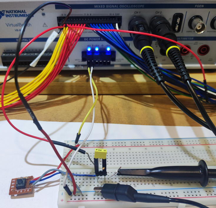 |
| Fig. 2. The push-button experiment monitored by the VB8012 instrument |
Fig. 3 shows the waveforms captured using C = 1.5 pF. Small value, as if it were not placed in the circuit, somewhat simulating all the parasitic capacitances of wires and instrument probes. Practically for all clicks several signal bounces are recorded in the event by the logic analyser when the signal is falling from high to low.
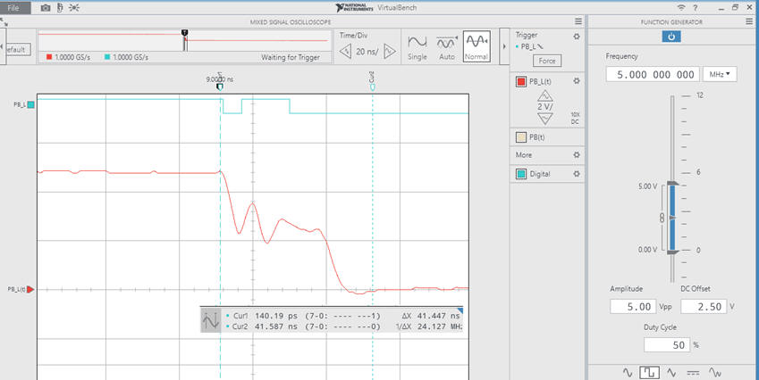 |
| Fig. 3. Example click waveforms using C = 1.5 pF. t = R·C = 15 ns. |
We can also represent, as in Fig. 4, the NOT gate input and output signals for the same C = 1.5 pF. Waveform shapes, event duration and bounces detected depends much on user click pressure on the button, and the quality and materials of the button itself.
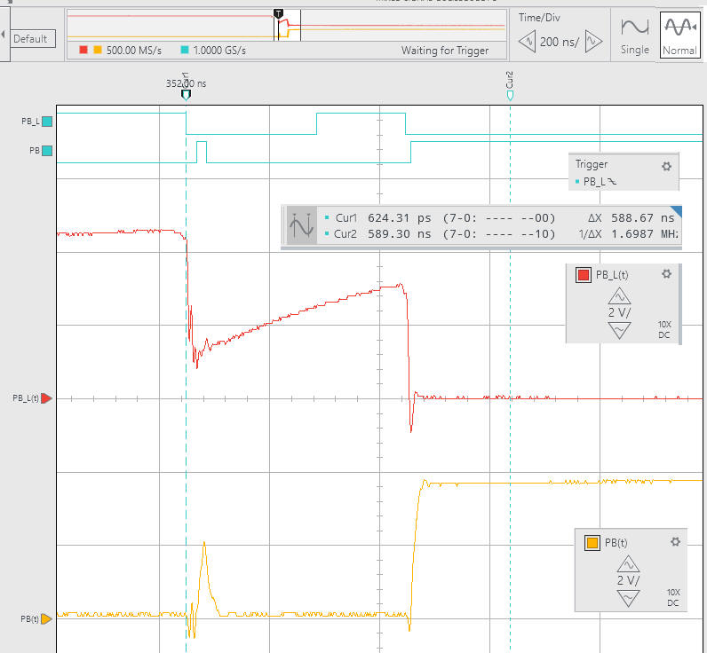 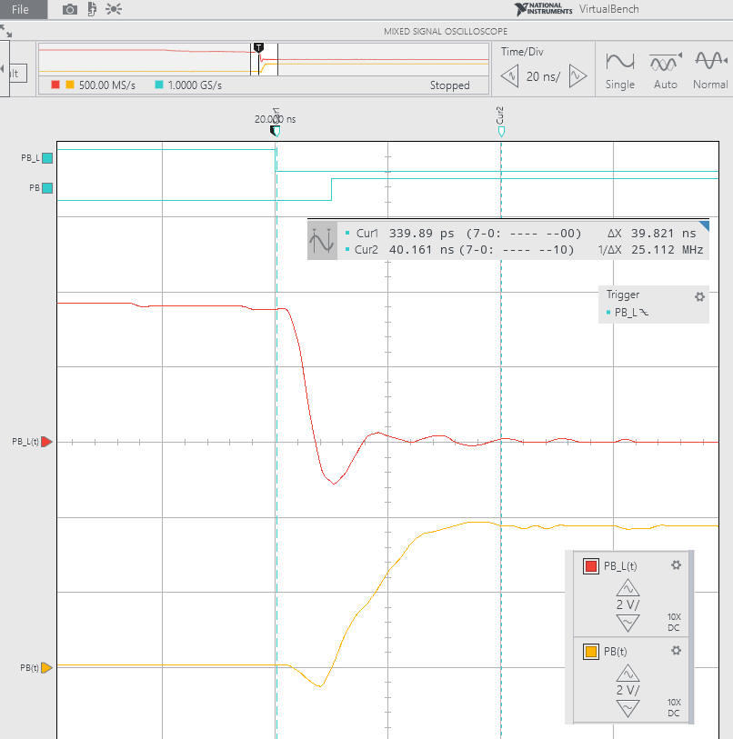 |
| Fig. 4. Example click waveforms when using the NOT gate SN74LS04, C = 1.5 pF. For every click captured, signals are different, and generally the NOT gate does a good job cleaning and sharpening the digital signal. NOT gate propagation delay from low to high is tPLH = 10 ns. |
Higher capacitors generate ringing waveforms. Even if the signal is much filtered, we cannot get rid of signal bounces.
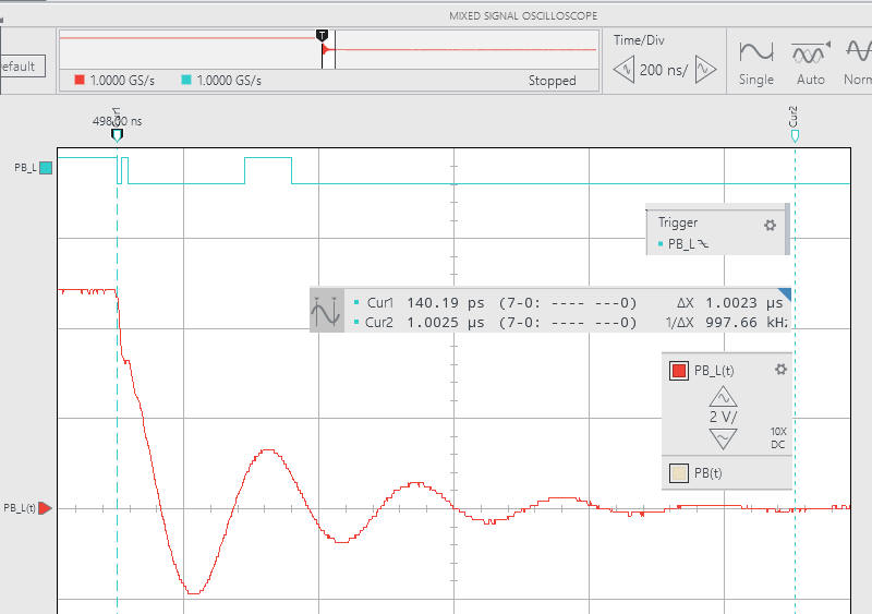  |
| Fig. 5. Example click waveforms using C = 10 nF. t = R·C = 100 ms. With and without the NOT gate. Generally, the inverter cleans and sharpens the active high signal generated. This concept can be reinforced repeating the experiment with an Schmitt trigger NOT gate type: SN74LS14. |
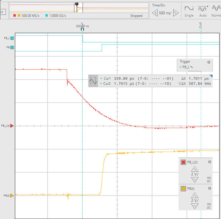 |
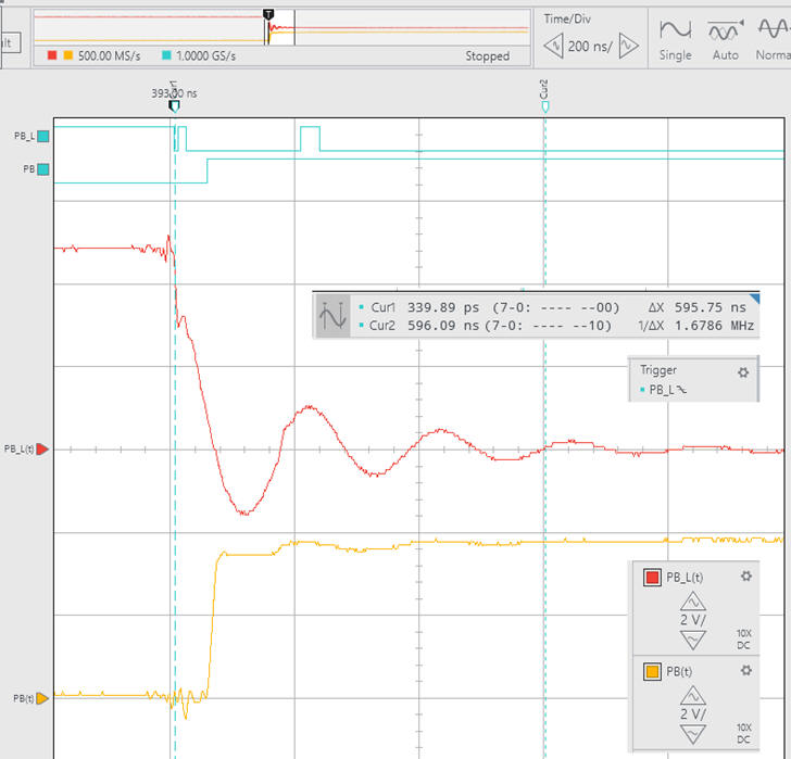
| Fig. 6. Example click waveforms using C = 1 mF. t = R·C = 10 ms. With the NOT gate. The event duration is 2 ms. |
Considering the results obtained using a simple RC filter, more elaborated button conditioning circuits using specialised gates (Schmitt trigger) can be inferred, for instance the circuit for the keys in the DE10-Lite board including the SN74LVC2G17 chip (Fig. 7).
And thus, for many applications requiring noise immunity and neat single event detection, additional digital synchronisers and debouncing filters based on FSM such the example presented in this tutorial, has to be included to generate clean digital events from push-buttons.
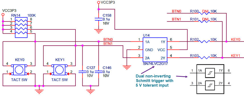 |
| Fig. 7. DE10-Lite circuits for debouncing key push-buttons. |
An interesting circuit, where we can see key bounce effects is the counter, as reported in LAB7 prototype. You can use the counter with and without the debouncing FSM attached to the CLK key input.
| Specifications | Planning | Developing | Testing (functional) | Testing (gate-level) | Prototype | 7. Report |
Follow this rubric for writing reports.
Push-button circuits. (A) debouncing filter, (B) synchroniser |
| 1. Specifications | Planning | Developing | Testing (functional) | Testing (gate-level) | Prototype | Report |
How to generate a clean single pulse synchronised with the system CLK from a noisy push-button? As shown in Fig. 1, we can add a second section to our previous debouncing filter to obtain such synchronous pulse. It can be used by any application as an external control input signal.
 |
| Fig. 1. Example application where a push-button is used to control operations. |
Generate a single synchronous pulse of TSYS_CLK duration to be used for commanding the application as an input PB. Chip2 Pulse_sync is another FSM. Determine how many states it will include representing a timing diagram. QA is the output from the Debouncing_filter above, a clean TS_CLK duration pulse.
Notes on the idea of the Pulse_sync.
| Specifications | 2. Planning | Developing | Testing (functional) | Testing (gate-level) | Prototype | Report |
FSM diagram and connections.
State diagram. State register. CC1 and CC2 truth table and flowchart.
| Specifications | Planning | 3. Developing | Testing (functional) | Testing (gate-level) | Prototype | Report |
VHDL translation
Quartus Prime project. Target FPGA chip.
RTL and technology view.
| Specifications | Planning | Developing | 4. Testing (functional) | Testing (gate-level) | Prototype | Report |
Testbench fixture.
ModelSim simulation.
| Specifications | Planning | Developing | Testing (functional) | 5. Testing (gate level) | Prototype | Report |
Gate-level simulation. Timing analyser. Timing parameters.
| Specifications | Planning | Developing | Testing (functional) | Testing (gate-level) | 6. Prototype | Report |
Mount the application in a given FPGA board. Consider the complete application in Fig. 1, for instance a 2 s timer triggered when clicking the push-button.
| Specifications | Planning | Developing | Testing (functional) | Testing (gate-level) | Prototype | 7. Report |
Follow this rubric for writing reports.
NOTE: Thinking about another section of this tutorial devoted to push-buttons, an interesting feature that can be used by many applications is the precision measuring of push-button clicks durations, let us say from 5 ms to 5 s, meaning 10-bit time resolution. How to implement such circuit and visualise results in ms in 7-segment displays?
| Home Term 26/27-Q1 Contact Products Electronic devices and companies Software Books Magazines Instruments DEE Library EETAC DEEL |

|
|
| Web activa des de 09/2001, @ F. J. Robert, Web editat amb Microsoft Expression Web 4. El contingut és un complement als materials d'estudi del curs Circuits i Sistemes Digitals disponibles al campus digital Atenea. Llicència:Reconeixement 4.0 Internacional de Creative Commons |