|
|
Bachelor's Degree in Telecommunications Systems and in Network Engineering |
|
|
|
||
|
|
Bin_BCD_16bit: plan C2 multiple VHDL files |
|
|
|
||
Structural design of a 16-bit binary radix-2 to BCD converter
1. Specifications
Design a 16-bit code converter from binary radix-2 to BCD using plan C2: hierarchical structure based on components of the same kind, for instance DM74185 and logic gates if necessary.
Bin_BCD_16bit has the symbol, truth table and example timing diagram represented in Fig. 1.
 |
|
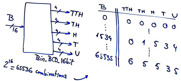
Fig. 1. Bin_BCD_16bit symbol and truth table. The truth table contain 2^16 = 65536 combinations. |
This is the article from Wikipedia where to find information on how to organise the circuit structure: the double dabble algorithm is used to convert radix-2 numbers into BCD.
2. Planning
Structural hierarchical plan C2, a plan based on interconnecting or chaining components (circuit expansion) and extra logic when necessary. The idea comes from the commercial chip 74185A datasheet as shown in Fig.3, an optimised version of the double dabble algorithm that performs additions in parallel. This the component DM74185 implemented using plan B. The same approach was as done in project Bin_BCD_9bit. We can use the schematic from the datasheet annotating all signals and referencing all the components. Be aware that inputs not used must be connected to '0'. Draw the component outputs that are not used, when instantiating the components, this outputs have to be left connected to a given signal name. For instance in Chip2: Y6 = D5.
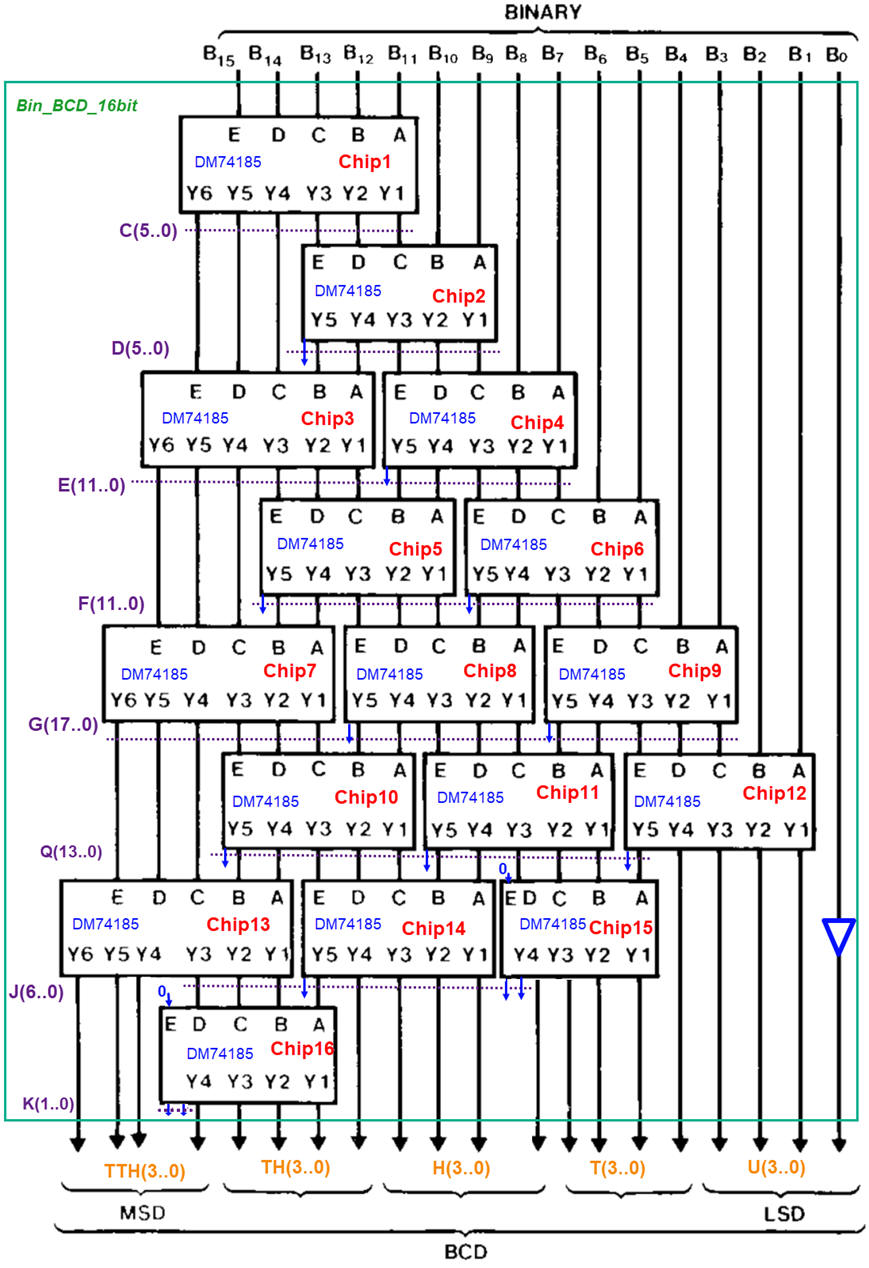 |
| Fig. 2. Bin_BCD_16bit architecture adapted from DM74185 datasheet and the tutorial Bin_BCD_9bit. We only have to change the circuit size to n = 16 and annotate the schematic to make it ready for VHDL. |
This is a two VHDL file project. Project location:
C:\CSD\P3\Bin_BCD_16bit\(files...)
3. Developing the project using EDA tools
Run a EDA project to synthesise the circuit. Let us target the DE10-Lite board MAX10 FPGA. This is the Bin_BCD_16bit.vhd circuit translation into VHDL from Fig. 2 above. We also have to include in the project the component DM74185 that is connected up to sixteen times.
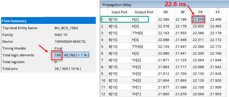
Fig. 3 shows the project summary .
 |
|
Fig. 3. Project summary showning that the converter is implemented in 196 logic elements. The propagation delay is 22.6 ns. |
FPGA resources used (logic elements). This project requires 196 logic elements.
 |
|
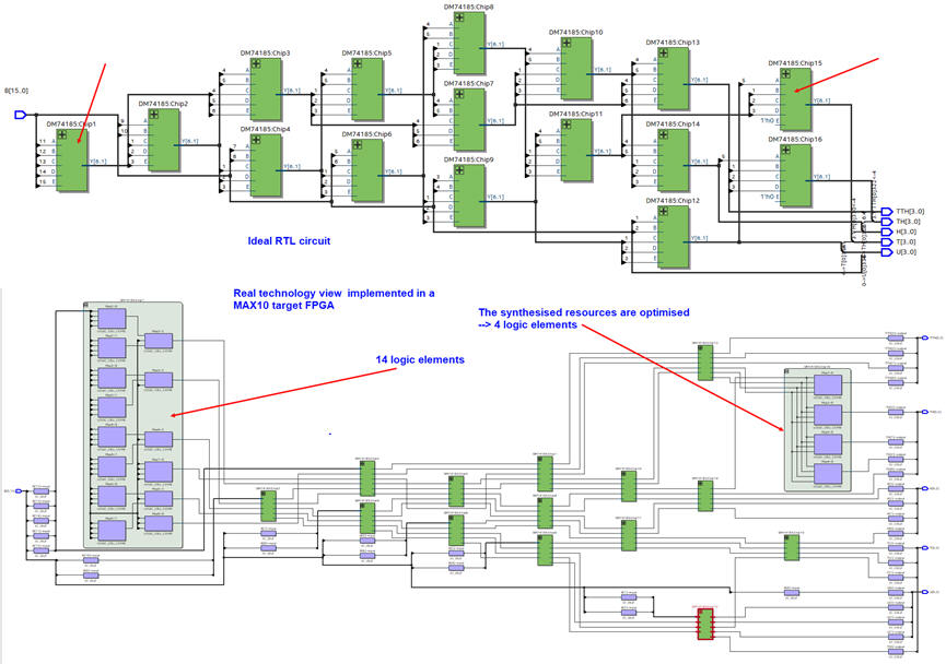
Fig. 3. RTL and technolgy schematics. |
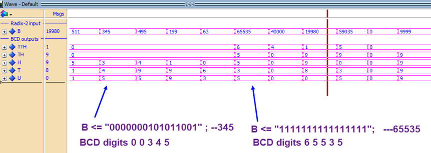
4. Testing and validating the design
We simply use the same stimulus process in the testbench fixture Bin_BCD_9bit enlarging the input numbers to 16-bit.
This is an example of testbench fixture translation to VHDL realdy for simulations in ModelSim: Bin_BCD_16bit_tb.vhd.
 |
|
Fig. 3. |
Once verified this device can be included in our library and it is ready to be used as a component in any project.
Note on comparing hardware designs: Annex A3 illustrates how radically different may be a circuit for the same entity and target FPGA (MAX10 10M50DAF484C7) but choosing two plans:
Plan C2. Our schematic in Fig.2, extacted from the classic TTL SN74185 1971 datasheet, is synthesised in 196 logic elements (< 1% of the chip capacity), generating a propagation delay of only tP = 22.6 ns
Plan B. From the internet Github, we can find and download the exact description as a behavioural flowchart of the double dabble algorithm for 16-bit as described in Wikipedia. When synthesised it uses 1733 logic elements (3% of the chip capacity), generating a propagation delay of tP = 146.7 ns
Designing efficient hardware requires a good comprehension of classic digital electronics; even today when it seems that everything fits in a single chip.
6. Report
At least five handwritten sheets of paper as usual in CSD. Follow this rubric for writing reports.
7. Prototyping
| Home Term 26/27-Q1 Contact Products Electronic devices and companies Software Books Magazines Instruments DEE Library EETAC DEEL |

|
|
| Web activa des de 09/2001, @ F. J. Robert, Web editat amb Microsoft Expression Web 4. El contingut és un complement als materials d'estudi del curs Circuits i Sistemes Digitals disponibles al campus digital Atenea. Llicència:Reconeixement 4.0 Internacional de Creative Commons |