|
|
Bachelor's Degree in Telecommunications Systems and in Network Engineering |
|
|
Programmable logic devices (target chips for synthesis and prototyping) |
||
sPLD, CPLD and FPGA (Chapters I and II)
Basic introduction to PLD and FPGA target chips. The Wikipedia PLD entry. Miniaturisation in electronic circuits.
1. sPLD: Simple PLD
The Wikipedia entry sPLD. We highly recommend you this video (18 min.).
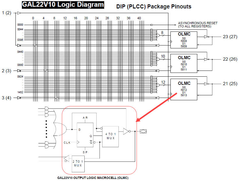 |
| Fig. 1. Example of logic array in sPLD. |
2. CPLD: Complex PLD
The Wikipedia entry CPLD. Logic functions are implemented in macrocell as PoS (1). Each logic block also includes a configurable flip-flop (FF) as the 1-bit memory cell (L5.2).
|
|
| Fig. 2. Example of CPLD logic cell or logic block. |
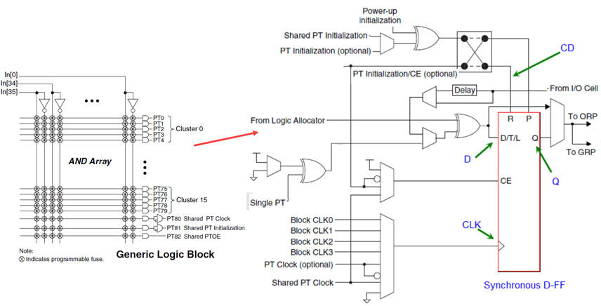
Hundreds or thousands of logic blocks configures the architecture of the CPLD. The chip also includes detached specialised blocks such RAM memories (L5.4).
|
|
| Fig. 2. Example of a CPLD. |

3. FPGA
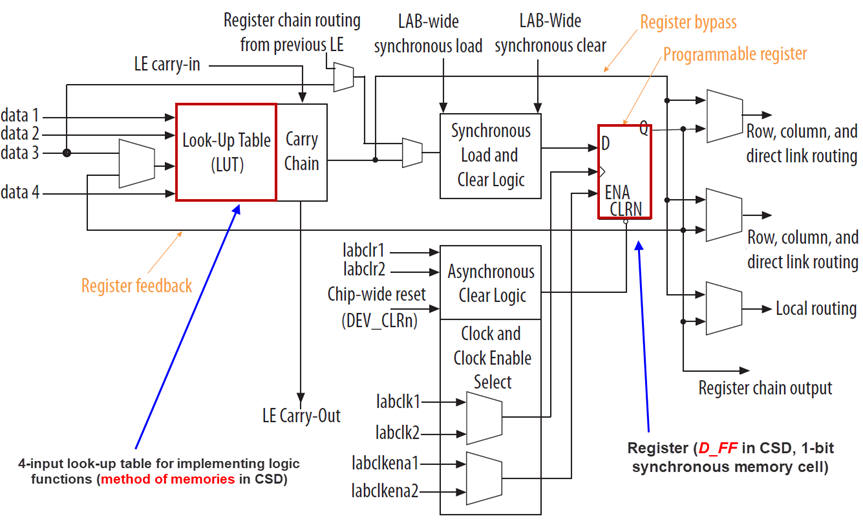
The Wikipedia entry FPGA. Logic functions are implemented using lookup tables (LUT), generally with a granularity of 4-input 1-bit RAM memory cells. The lecture L5.4 proposes the idea on how to implement logic functions using ROM.
We highly recommend you this video (20 min.). A kind of a perfect introduction to modern FPGA devices.
The high-level introduction field-programmable gate arrays "FPGA Explained" from Digilent.
|
|
| Fig. 3. FPGA logic element. Ref. Intel MAX10 10M50DAF484C7G. |
Prototyping boards
We are performing introductory lab experiments using the FPGA DE10-Lite board.
|
|
| Fig. 4. The DE10-Lite structure. |

Books
It is a good time for reading a book chapter on programmable logic devices. For instance, Chapter 11 in "INTRODUCTION TO LOGIC CIRCUITS & LOGIC DESIGN WITH VHDL", Brock J. LaMeres, 2nd edition, Springer, 2019, https://doi.org/10.1007/978-3-030-12489-2, available at the UPC library. Indeed, any book on digital logic explains very well what is a programmable logic device able to implement combinational and sequential logic functions.
These are other recommended readings (1) (2) on sPLD, CPLD and FPGA.
| Home Term 26/27-Q1 Contact Products Electronic devices and companies Software Books Magazines Instruments DEE Library EETAC DEEL |

|
|
| Web activa des de 09/2001, @ F. J. Robert, Web editat amb Microsoft Expression Web 4. El contingut és un complement als materials d'estudi del curs Circuits i Sistemes Digitals disponibles al campus digital Atenea. Llicència:Reconeixement 4.0 Internacional de Creative Commons |