|
|
Bachelor's Degree in Telecommunications Systems and in Network Engineering |
|
|
ROM/RAM method for implementing logic functions |
||
The method of ROM memory cells for implementing logic functions is referred as the 14th method in our list of strategies for designing combinational circuits.
1. Specifications
Example circuit. Invent the combinational circuit described by the truth table Fig. 1 using the method of memories. Determine the values to be saved in the ROM memory 8x4. Develop and test your circuit.
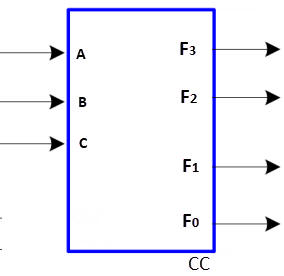 |
F3 = f(A, B, C) = Sm(2, 3, 5, 6, 7) F2 = f(A, B, C) = Sm(0, 1, 2, 6) F1 = f(A, B, C) = Sm(2, 3, 4, 6, 7) F0 = f(A, B, C) = Sm(0, 1, 4, 6) |
|
Fig. 1. Example of a combinational circuit to be solved by the method of ROM memories. |
|
2. Plan
As a first step, the truth table of the CC circuit has to be filled in. The truth table values are written in the ROM memory component.
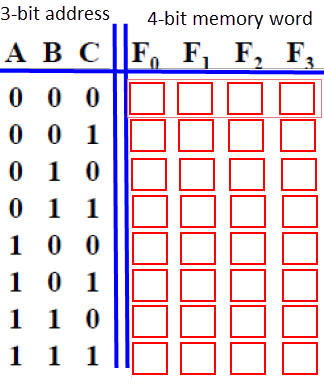 |
Fig. 2. Fill in the 8 rows of the truth table; it will be the ROM content for each addresses. |
As deduced inspecting the truth table, a ROM_8x4 component is required in this CC based on plan C2.
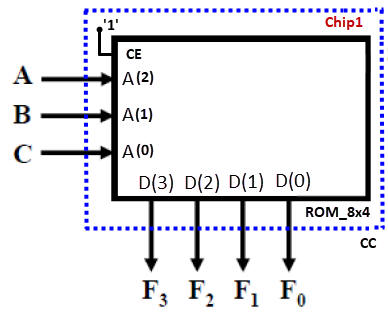 |
Fig. 3. Example of a 23x4 memory which allows the implementation of 4 logic functions Fi = f(A, B, C) using plan C2. |
3. Develop
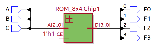
Write the top VHDL file CC.vhd and run an EDA synthesis tool including the ROM_8x4.vhd component. Inspect the final RTL and technology schematics. Note: in this file, outputs are interpreted as individual wires instead of a vector.
 |
|
Fig. 4. RTL schematic. |
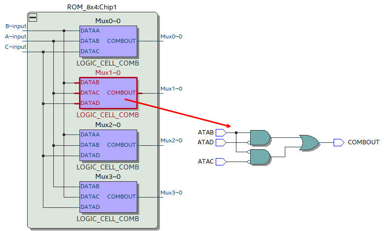
Fig 5 shows the technology schematic used in a Cyclone IV FPGA chip to materialise the ROM device. Because we have defined a one-time programmable (OTP) ROM that is written in the synthesis/manufacturing process itself, it is based on simple combinational logic (LOGIC_CELL_COMB) and registers type D_FF are not required.
 |
|
Fig. 5. Technology view representation. |
An interesting exercise at this level is solving the same CC circuit in PoS using plan A from the circuit's truth table in Minilog and compare RTL and technology views.
(Optional) An also another more complex project out of CSD content is solving the same circuit using RAM synthesised for a specific target chip.
4. Test
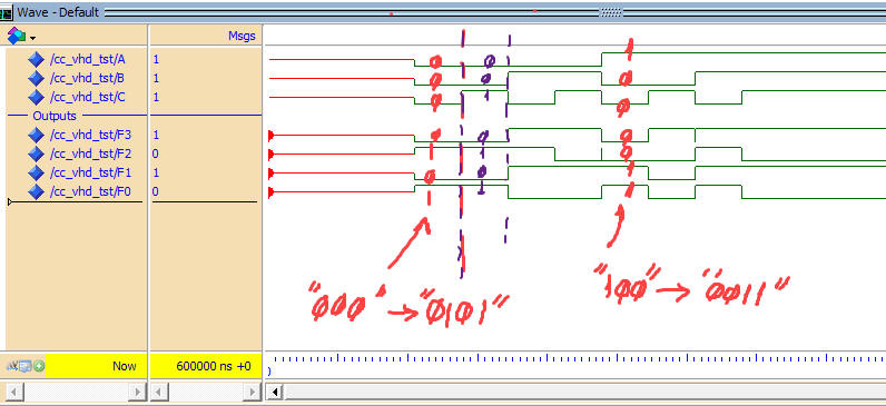
This is an example testbench file in VHDL CC_tb.vhd to test the truth table.
 |
|
Fig. 6. Example of testing the truth table. |
Another tutorial exercise
Another example project that includes a ROM component and logic gates: Hex_7seg_decoder.
| Home Term 26/27-Q1 Contact Products Electronic devices and companies Software Books Magazines Instruments DEE Library EETAC DEEL |

|
|
| Web activa des de 09/2001, @ F. J. Robert, Web editat amb Microsoft Expression Web 4. El contingut és un complement als materials d'estudi del curs Circuits i Sistemes Digitals disponibles al campus digital Atenea. Llicència:Reconeixement 4.0 Internacional de Creative Commons |