

|
Bachelor's Degree in Telecommunications Systems and Network Engineering |

|
Chapter 2 problems |
- D2.22 - |
Bit-pattern generator (FPGA-VHDL) |
A digital pattern generator is a piece of electronic test equipment or software used to generate digital electronic stimuli (ref.). The testing signals can be very specialised like video bars for a TV, serial transmission standards or logic signals for computer chips.
Fig. 1 shows how this device is modelled in Proteus as an instrument to drive one and zero sequences for verifying the truth table of the Chip2 device under test.
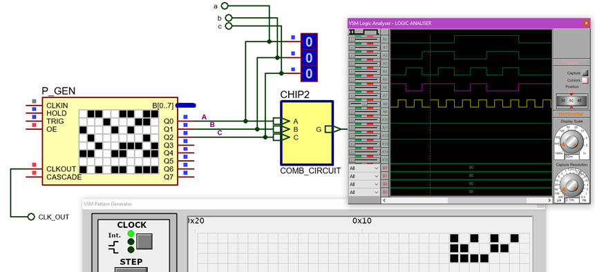 |
| Fig. 1. Example of pattern generator instruments. |
Fig. 2 shows how the Patterns application can be used by the Analog Discovery 2 compact instrument driven by WaveForms software to generate a random binary sequence.

 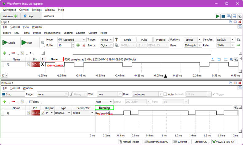 |
| Fig. 2. Example of a random binary pattern generated by Waveforms and Discovery 2 compact instrument. |
Fig. 3 shown a schematic (ref.) to design a classic TV pattern generator using specialised integrated circuits such the ZNA234.
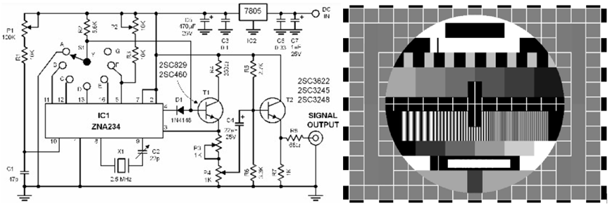 |
| Fig. 3. Example of a vintage black and white TV test pattern generator based on the ZNA234 chip. |
1. Specifications
Design a bit pattern generator as shown in Fig. 4. It will serialise 12-bit of data that the user will input in two steps along with some transmission configuration bits.
Four transmission speeds (SYS_CLK frequency) will be configured using the two CF bits.
M bit will set single frame or repeated transmission frames.
S bit will determine how to transmit: 12-bits of user raw data, or a byte using serial standard.
After the initial CD_L signal, the device will wait for two start pattern (SP) push-button clicks. The first click will be for inputting the high byte of Din(15..8); the second click will be for inputting the low byte Din(7..0).
The green LED (LED_g) will be lighting while waiting for the second SP click. The red LED (LED_r) will be lighting while transmitting.
CLK signals are derived from an external 50 MHz quartz oscillator and it is also available as the output CLK_out.
To convey and serialise the data to a single output Serial_out, the key component is a datapath containing a 12-bit left-shift register, connected also as a rotator for continuous transmission.
The same project designed programming a μC is in D3.22.
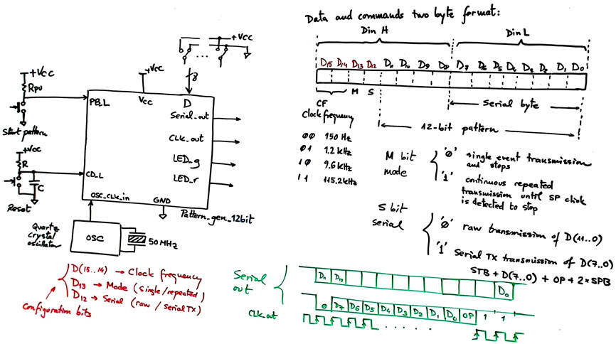 |
| Fig. 4. Symbol and main features for configuring bit sequences. |
Some example patterns are represented in Fig. 5.
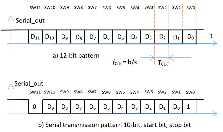 |
| Fig. 5. Bit pattern examples. |
Discuss the given specifications. Find laboratory instruments of this kind. Find applications for such bit generator. How to characterise digital transmissions using eye diagrams, pattern generators and oscilloscopes? Some references: 1, 2, 3.
Currently, we will organise a standard dedicated processor in three design phases to complete the specifications. However, beyond the current project, an upgraded circuit can be proposed to store and generate larger bit pattern transmissions using RAM chips. Another feature may be to generate random patterns.
2. Planning ideas
Design phase #1: basic FSM
Step #1: Start pulse
We can start the circuit conception by discussing how the start pattern push-button can be interfaced to the generator. Fig. 6 proposes an interface circuit. Mechanical switches and buttons generate noisy signals that must be filtered to be used correctly in digital circuits. On one hand, signal bounces can be suppressed using Chip1, a Debouncing_filter. On the other hand, we can generate a single synchronised pulse to drive the pattern generator at its SYS_CLK frequency using Chip2 running the three-state FSM Pulse_Sync.
 |
| Fig. 6. Signal filtering and synchronisation. |
Complete the tutorial Pulse_Sync and check that it works using a VHDL testbench.
Project location:
C:\CSD\P6\Single_Pulse_gen\(files)
Step #2: Counter_mod12 with synchronous reset
Use plan C2 and our standard Counter_mod16 to implement the Counter_mod12 with a synchronous reset that is used for counting the 12-bit serialisation.
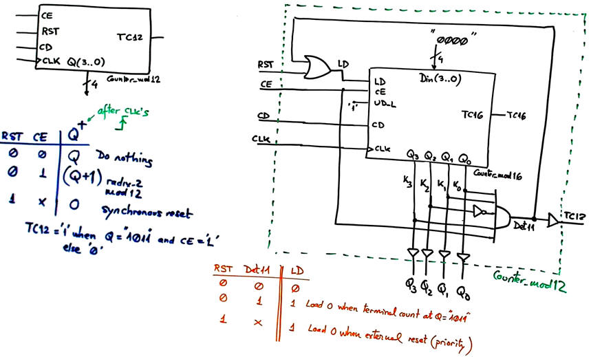 |
| Fig. 7. Symbol, function table and proposed architecture for the Counter_mod12. used as Chip2 in Fig. 9. |
Project location:
C:\CSD\P7\Counter_mod12\(files)
Step #3: Datapath components
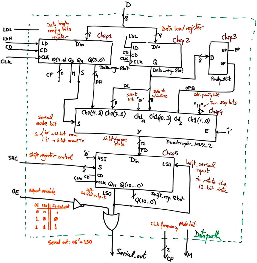
To control operations and serialise data to generate the specified user patterns, several circuits are required in the datapath: data and shift registers, a multiplexer and an odd-parity generator.
 |
|
Fig. 8. Proposed datapath. The configuration bit S selects between the raw 12-bit data and the formatted 8-bit serial data. |
Project location:
C:\CSD\P7\Datapath\(files)
Complete the datapath translating the schematics into VHDL using plan C2.
Design phase #2: FSM + datapath
The FSM will control how and when the data is serialised, as shown in Fig. 9. The structure and organisation of this device are conceived as a microcontroller peripheral that can be commanded by software instructions, rather than user clicks and switches, if required. The Chip2 counter will allow 12-bit shifting sequences. Chip4 generates the external LED indicators and also the datapath control signals that will process the input data.
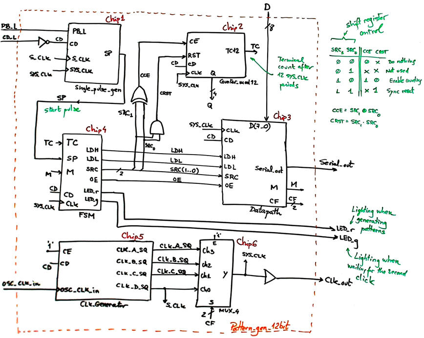 |
| Fig. 9. Pattern generator dedicated processor to comply with the specifications. Chips 5 and 6 will be added in the next design phase. |
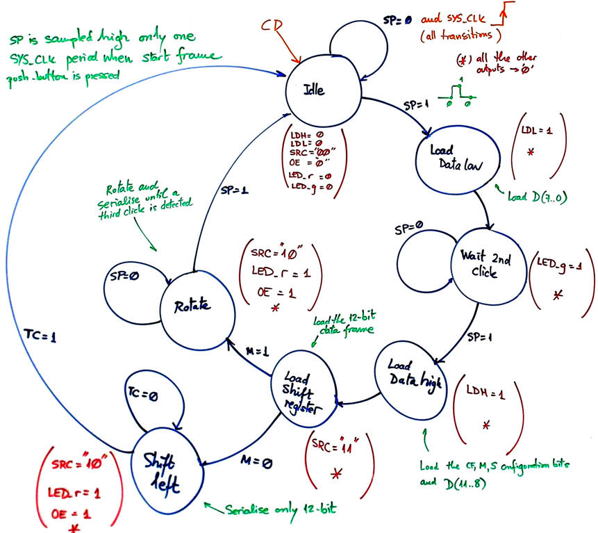
And now, the idea to run the system is to propose a state diagram for Chip4, the FSM to control the processor's datapath, as shown in Fig. 10.
 |
|
Fig. 10. Control unit FSM state diagram. |
Adapt the FSM architecture to this problem, naming and connecting all signals and inputs and outputs.
Draw the state register memory based on D_FF and deduce the number of D_FF required when encoding the machine using the following options:
Option #1: radix-2 (sequential)
Option #2: Gray
Option #3: Johnson
Option #4: one-hot
Draw the CC2 truth table to obtain the circuit's outputs and its equivalent flowchart behavioural interpretation (plan B).
Draw the CC1 truth table to obtain the circuit's state transitions and its equivalent flowchart behavioural interpretation (plan B).
Project location:
C:\CSD\P8\Pattern_gen_12bit\(files)
Write the FSM VHDL file.
Start a Quartus Prime synthesis project for one of the following programmable target chips:
Option #1: Cyclone IV EP4CE115F29C7
Option #2: MAX II EPM2210F324C3
Option #3: MAX 10 10M50DAF484C7 (*)
(*) Remember that this chip does not generate sdo delay files, thus use another one when gate-level simulations are required.
Inspect and annotate the RTL and technology views. Check the number of D_FF synthesised in this application.
Generate a VHDL testbench fixture schematic using two CLK signals.
 |
|
Fig. 11. Testbench fixture. What inputs, outputs and internal signals are to be monitored? |
Run functional simulations to verify your design. Visualise as well in the wave timing diagram the internal states.
Run gate-level simulations to measure the propagation time CLK to output (tCO). Measure the minimum TCLK period or the maximum frequency of operation of the FSM.
Design phase #3: CLK_Generator
Design the CLK generator circuit from a 50 MHz quartz crystal oscillator to obtain all the clocking signals required to drive the application enhancing the pattern generator circuit in Fig. 9 with Chip5 and Chip6.
Deduce the number of D_FF that the full project Pattern_gen_12bit will require.
Project location: C:\CSD\P8\Pattern_gen_12bit\(files)
The options for the SYS_CLK are chosen from standard serial bit rates:

Option #1: fS_CLK = 150 Hz; fSYS_CLK = 150 Hz, 1.2 kHz, 9.6 kHz, 115.2 kHz
Option #2: fS_CLK = 300 Hz; fSYS_CLK = 300 Hz, 1.8 kHz 7.2 kHz, 57.6 kHz
Option #3: fS_CLK = 134 Hz; fSYS_CLK = 134 Hz, 2.4 kHz, 14.4 kHz, 128 kHz
| Home Term 26/27-Q1 Contact Products Electronic devices and companies Software Books Magazines Instruments DEE Library EETAC DEEL |

|

|
| Web activa des de 09/2001, @ F. J. Robert, Web editat amb Microsoft Expression Web 4. El contingut és un complement als materials d'estudi del curs Circuits i Sistemes Digitals disponibles al campus digital Atenea. Llicència:Reconeixement 4.0 Internacional de Creative Commons |